EVAL-AD7689EDZ Analog Devices Inc, EVAL-AD7689EDZ Datasheet - Page 23
EVAL-AD7689EDZ
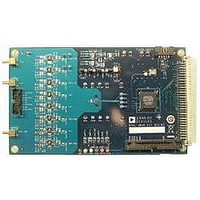
Manufacturer Part Number
EVAL-AD7689EDZ
Description
BOARD EVAL AD7689
Manufacturer
Analog Devices Inc
Series
PulSAR®r
Specifications of EVAL-AD7689EDZ
Number Of Adc's
1
Number Of Bits
16
Sampling Rate (per Second)
250k
Data Interface
Serial
Inputs Per Adc
8 Single Ended
Input Range
±VREF
Power (typ) @ Conditions
12.5mW @ 250kSPS, 5 V
Voltage Supply Source
Single Supply
Operating Temperature
-40°C ~ 85°C
Utilized Ic / Part
AD7689
Silicon Manufacturer
Analog Devices
Application Sub Type
ADC
Kit Application Type
Data Converter
Silicon Core Number
AD7689
Lead Free Status / RoHS Status
Lead free / RoHS Compliant


DIGITAL INTERFACE
The AD7682/AD7689 use a simple 4-wire interface and are
compatible with SPI, MICROWIRE™, QSPI™, digital hosts,
and DSPs, for example, Blackfin® ADSP-BF53x, SHARC®,
ADSP-219x, and ADSP-218x.
The interface uses the CNV, DIN, SCK, and SDO signals and
allows CNV, which initiates the conversion, to be independent
of the readback timing. This is useful in low jitter sampling or
simultaneous sampling applications.
A 14-bit register, CFG[13:0], is used to configure the ADC for
the channel to be converted, the reference selection, and other
components, which are detailed in the Configuration Register,
CFG, section.
When CNV is low, reading/writing can occur during conversion,
acquisition, and spanning conversion (acquisition plus conver-
sion), as detailed in the following sections. The CFG word is
updated on the first 14 SCK rising edges, and conversion results
are output on the first 15 (or 16 if busy mode is selected) SCK
falling edges. If the CFG readback is enabled, an additional
14 SCK falling edges are required to output the CFG word
associated with the conversion results with the CFG MSB
following the LSB of the conversion result.
A discontinuous SCK is recommended because the part is
selected with CNV low, and SCK activity begins to write a new
configuration word and clock out data.
Note that in the following sections, the timing diagrams indicate
digital activity (SCK, CNV, DIN, SDO) during the conversion.
However, due to the possibility of performance degradation,
digital activity should occur only prior to the safe data reading/
writing time, t
correction circuitry that can correct for an incorrect bit during
this time. From t
conversion results may be corrupted. The user should configure
the AD7682/AD7689 and initiate the busy indicator (if desired)
prior to t
SCK or DIN transitions near the sampling instant. Therefore, it
is recommended to keep the digital pins quiet for approximately
20 ns before and 10 ns after the rising edge of CNV, using a
discontinuous SCK whenever possible to avoid any potential
performance degradation.
READING/WRITING DURING CONVERSION, FAST
HOSTS
When reading/writing during conversion (n), conversion
results are for the previous (n − 1) conversion, and writing the
CFG register is for the next (n + 1) acquisition and conversion.
After the CNV is brought high to initiate conversion, it must be
brought low again to allow reading/writing during conversion.
Reading/writing should only occur up to t
time is limited, the host must use a fast SCK.
DATA
. It is also possible to corrupt the sample by having
DATA
DATA
, because the AD7682/AD7689 provide error
to t
CONV
, there is no error correction and
DATA
and, because this
Rev. B | Page 23 of 32
The SCK frequency required is calculated by
The time between t
activity should not occur, or sensitive bit decisions may be
corrupt.
READING/WRITING AFTER CONVERSION, ANY
SPEED HOSTS
When reading/writing after conversion, or during acquisition
(n), conversion results are for the previous (n − 1) conversion,
and writing is for the (n + 1) acquisition.
For the maximum throughput, the only time restriction is that
the reading/writing take place during the t
For slow throughputs, the time restriction is dictated by the
throughput required by the user, and the host is free to run at
any speed. Thus for slow hosts, data access must take place
during the acquisition phase.
READING/WRITING SPANNING CONVERSION, ANY
SPEED HOST
When reading/writing spanning conversion, the data access starts
at the current acquisition (n) and spans into the conversion (n).
Conversion results are for the previous (n − 1) conversion, and
writing the CFG register is for the next (n + 1) acquisition and
conversion.
Similar to reading/writing during conversion, reading/writing
should only occur up to t
the only time restriction is that reading/writing take place
during the t
For slow throughputs, the time restriction is dictated by the
user’s required throughput, and the host is free to run at any
speed. Similar to reading/writing during acquisition, for slow
hosts, the data access must take place during the acquisition
phase with additional time into the conversion.
Note that data access spanning conversion requires the CNV to
be driven high to initiate a new conversion, and data access is
not allowed when CNV is high. Thus, the host must perform
two bursts of data access when using this method.
CONFIGURATION REGISTER, CFG
The AD7682/AD7689 use a 14-bit configuration register
(CFG[13:0]), as detailed in Table 10, to configure the inputs,
the channel to be converted, the one-pole filter bandwidth,
the reference, and the channel sequencer. The CFG register is
latched (MSB first) on DIN with 14 SCK rising edges. The CFG
update is edge dependent, allowing for asynchronous or
synchronous hosts.
f
SCK
≥
ACQ
Number
+ t
DATA
DATA
t
_
DATA
time.
SCK
and t
DATA
_
CONV
. For the maximum throughput,
Edges
is a safe time when digital
AD7682/AD7689
ACQ
(minimum) time.
Related parts for EVAL-AD7689EDZ
Image
Part Number
Description
Manufacturer
Datasheet
Request
R


Part Number:
Description:
BOARD EVAL FOR SI270X-A
Manufacturer:
Silicon Laboratories Inc
Datasheet:

Part Number:
Description:
BUCK CONV REF DESIGN KIT IP1201
Manufacturer:
International Rectifier
Datasheet:
Part Number:
Description:
BOARD DEMO SYNC DUAL BUCK CNVTER
Manufacturer:
International Rectifier
Datasheet:
Part Number:
Description:
BOARD DEMO SYNC BUCK CONVETER
Manufacturer:
International Rectifier
Datasheet:

Part Number:
Description:
EVALBOARD/EB Omnidirectional microphone - Analog
Manufacturer:
Analog Devices
Datasheet:
Part Number:
Description:
EVALBOARD/EB Omnidirectional microphone - Analog
Manufacturer:
Analog Devices
Datasheet:


Part Number:
Description:
BOARD EVAL LED DRIVER LT3756
Manufacturer:
Linear Technology
Datasheet:

Part Number:
Description:
BOARD EVAL FOR AD7741/7742
Manufacturer:
Analog Devices Inc
Datasheet:

Part Number:
Description:
±1.7g Dual-Axis IMEMS Accelerometer Evaluation Board
Manufacturer:
Analog Devices Inc
Datasheet:

Part Number:
Description:
IC MULTIPLIER ANALOG 8-SOIC T/R
Manufacturer:
Analog Devices Inc
Datasheet:

Part Number:
Description:
IC ANALOG MULTIPLIER 8-DIP
Manufacturer:
Analog Devices Inc
Datasheet:
Part Number:
Description:
IC ANALOG MULTIPLIER 8-SOIC
Manufacturer:
Analog Devices Inc
Datasheet:
Part Number:
Description:
IC ANALOG MULTIPLIER 8-DIP
Manufacturer:
Analog Devices Inc
Datasheet: