EVAL-AD7689EDZ Analog Devices Inc, EVAL-AD7689EDZ Datasheet - Page 30
EVAL-AD7689EDZ
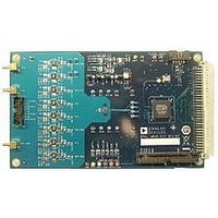
Manufacturer Part Number
EVAL-AD7689EDZ
Description
BOARD EVAL AD7689
Manufacturer
Analog Devices Inc
Series
PulSAR®r
Specifications of EVAL-AD7689EDZ
Number Of Adc's
1
Number Of Bits
16
Sampling Rate (per Second)
250k
Data Interface
Serial
Inputs Per Adc
8 Single Ended
Input Range
±VREF
Power (typ) @ Conditions
12.5mW @ 250kSPS, 5 V
Voltage Supply Source
Single Supply
Operating Temperature
-40°C ~ 85°C
Utilized Ic / Part
AD7689
Silicon Manufacturer
Analog Devices
Application Sub Type
ADC
Kit Application Type
Data Converter
Silicon Core Number
AD7689
Lead Free Status / RoHS Status
Lead free / RoHS Compliant


AD7682/AD7689
APPLICATION HINTS
LAYOUT
The printed circuit board (PCB) that houses the AD7682/AD7689
should be designed so that the analog and digital sections are
separated and confined to certain areas of the board. The pinout of
the AD7682/AD7689, with all its analog signals on the left side
and all its digital signals on the right side, eases this task.
Avoid running digital lines under the device because these
couple noise onto the die unless a ground plane under the
AD7682/AD7689 is used as a shield. Fast switching signals,
such as CNV or clocks, should not run near analog signal
paths. Avoid crossover of digital and analog signals.
At least one ground plane should be used. It can be common or
split between the digital and analog sections. In the latter case,
the planes should be joined underneath the AD7682/AD7689.
The AD7682/AD7689 voltage reference input REF has a
dynamic input impedance and should be decoupled with
minimal parasitic inductances. This is done by placing the
Rev. B | Page 30 of 32
reference decoupling ceramic capacitor close to, ideally right up
against, the REF and GND pins and connecting them with wide,
low impedance traces.
Finally, the power supplies VDD and VIO of the AD7682/
AD7689 should be decoupled with ceramic capacitors, typically
100 nF, placed close to the AD7682/AD7689, and connected
using short, wide traces to provide low impedance paths and to
reduce the effect of glitches on the power supply lines.
EVALUATING AD7682/AD7689 PERFORMANCE
Other recommended layouts for the AD7682/AD7689 are
outlined in the documentation of the evaluation board for the
AD7682/AD7689 (EVAL-AD7682EDZ/EVAL-AD7689EDZ).
The evaluation board package includes a fully assembled and
tested evaluation board, documentation, and software for
controlling the board from a PC via the converter and evaluation
development data capture board, EVAL-CED1Z.
Related parts for EVAL-AD7689EDZ
Image
Part Number
Description
Manufacturer
Datasheet
Request
R


Part Number:
Description:
BOARD EVAL FOR SI270X-A
Manufacturer:
Silicon Laboratories Inc
Datasheet:

Part Number:
Description:
BUCK CONV REF DESIGN KIT IP1201
Manufacturer:
International Rectifier
Datasheet:
Part Number:
Description:
BOARD DEMO SYNC DUAL BUCK CNVTER
Manufacturer:
International Rectifier
Datasheet:
Part Number:
Description:
BOARD DEMO SYNC BUCK CONVETER
Manufacturer:
International Rectifier
Datasheet:

Part Number:
Description:
EVALBOARD/EB Omnidirectional microphone - Analog
Manufacturer:
Analog Devices
Datasheet:
Part Number:
Description:
EVALBOARD/EB Omnidirectional microphone - Analog
Manufacturer:
Analog Devices
Datasheet:


Part Number:
Description:
BOARD EVAL LED DRIVER LT3756
Manufacturer:
Linear Technology
Datasheet:

Part Number:
Description:
BOARD EVAL FOR AD7741/7742
Manufacturer:
Analog Devices Inc
Datasheet:

Part Number:
Description:
±1.7g Dual-Axis IMEMS Accelerometer Evaluation Board
Manufacturer:
Analog Devices Inc
Datasheet:

Part Number:
Description:
IC MULTIPLIER ANALOG 8-SOIC T/R
Manufacturer:
Analog Devices Inc
Datasheet:

Part Number:
Description:
IC ANALOG MULTIPLIER 8-DIP
Manufacturer:
Analog Devices Inc
Datasheet:
Part Number:
Description:
IC ANALOG MULTIPLIER 8-SOIC
Manufacturer:
Analog Devices Inc
Datasheet:
Part Number:
Description:
IC ANALOG MULTIPLIER 8-DIP
Manufacturer:
Analog Devices Inc
Datasheet: