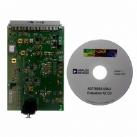
EVAL-AD7766-1EDZ Analog Devices Inc, EVAL-AD7766-1EDZ Datasheet - Page 4

EVAL-AD7766-1EDZ
Manufacturer Part Number
EVAL-AD7766-1EDZ
Description
BOARD EVAL AD7766-1 64KSPS 111DB
Manufacturer
Analog Devices Inc
Specifications of EVAL-AD7766-1EDZ
Number Of Adc's
1
Number Of Bits
24
Sampling Rate (per Second)
64k
Data Interface
Serial
Inputs Per Adc
1 Differential
Input Range
±VREF
Power (typ) @ Conditions
10.5mW @ 64kSPS
Voltage Supply Source
Analog and Digital
Operating Temperature
-40°C ~ 105°C
Utilized Ic / Part
AD7766-1
Lead Free Status / RoHS Status
Lead free / RoHS Compliant
EVAL-AD7766/66-1/66-2
There are a further 10 solder link options for various functions. These link options are outlined in Table 2. All solder links are set so that
the user can plug and play the evaluation board direct. The default settings lists the settings for the AD7766/-1/-2 evaluation board for
operation with the CED board and are listed in the right hand column of the table.
Table 2.Solder Link Option Functions
Link No.
SL1
SL2
SL3
SL4
SL5
SL6
SL8
SL9
Position
A
B
A
B
A
B
A
B
A
B
C
A
B
A
B
C
D
A
B
Function
Selects the source of the SCLK applied to the AD7766/-1/-2
Selects CED as SCLK source.
In stand-alone operation an external SCLK can be applied to the AD7766/-1/-2 device by means of J8
Selects the source of the CS signal to be applied to AD7766/-1/-2 device.
Selects CED as CS source.
In stand-alone operation an external CS can be applied to the AD7766/-1/-2 device by means of J5
Selects the source of the signal applied to SDI (serial data input) pin of the AD7766/-1/-2, used in
daisy-chain applications.
Ties SDI pin to 2.5V volts logic high default setting for SDI pin when using the AD7766/-1/-2 devices
singly.
Allows user to input data from another AD7766/-1/-2 device to verify daisy-chain functionality.
Selects the path of the DRDY output from the AD7766/-1/-2 device
Use for CED board. Routes the DRDY signal from the AD7766/-1/-2 device to the CED control board
via the 96-way connector.
In stand-alone operation the DRDY can be routed to the SMB connector J11.
Selects the MCLK source applied to the AD7766/-1/-2 device.
External MCLK source applied to SMB connector J7 is applied to the AD7766/-1/-2 MCLK pin.
On board crystal oscillator, Y1 output is routed to the AD7766/-1/-2 applying a 1Mhz clock to the
MCLK pin (a 1Mhz MCLK signal allows the AD7766/-1/-2 devices to operate with an output data rate
of 128 kHz, 64 kHz, and 32 kHz respectively). Placing 1KΩ resistors in positions R43 and R23 allows the
user to potentially divide the 5V output of the crystal to 2.5V as per the V
AD7766/-1/-2 evaluation board.
Applies the 1.024Mhz MCLK signal created by the CED board to be applied to the AD7766/-1/-2 MCLK
pin. Enables the AD7766/-1/-2 device to operate at the maximum output data rate.
Routes the Serial Data Output (SDO) to the CED board or the SMB connector J9.
Routes the SDO signal to J9, the SMB connector marked “SDO” allowing data to be acquired by an
external element in stand-alone mode.
Routes the SDO signal to the 96-way connector so that data can be acquired by the CED control
board.
Selects the source of the voltage applied to the V
A 2.5V supply created by the CED board is supplied to the AD7766/-1/-2 V
Allows the user to apply an external V
pin.
Applies the 2.5V supply created by the ADP3330-2.5 regulator (U11) to the AD7766/-1/-2 V
Allows a 2.5V supply to be applied to the AD7766/-1/-2 VDRIVE pin from a star point at the output of
the ADP3330-2.5 regulator (U8) which creates the 2.5V supply for the DVDD pin. When using this
option, ensure that the resistive link between AD7766/-1/-2 side of R7 and the D pad of SL8 is
shorted.
Selects the 2.5V path that is routed to the AVDD1 pin of the AD7766/-1/-2 device (pin 1).
Allows the AD7766/-1/-2 to be run off one 2.5V regulator by linking the pin to the DVDD star point on
the AD7766/-1/-2 side of the resistor R7. Using this option requires that the resistive placeholder
between pad A of SL9 and the DVDD star point (device side of R7) is shorted.
Routes the 2.5V supply created by the ADP3330-2.5 device (U9) to the AVDD1 pin of the AD7766/-1/-
2 device.
Rev. PrB | Page 4 of 24
DRIVE
supply (via the J13 connector) to the AD7766/-1/-2 V
DRIVE
pin.
Preliminary Technical Data
DRIVE
DRIVE
voltage default on the
pin.
DRIVE
DRIVE
pin.
Default /
Packaged
Setting
A
A
B
A
C
B
C
B


