EVAL-AD7766-1EDZ Analog Devices Inc, EVAL-AD7766-1EDZ Datasheet - Page 17
EVAL-AD7766-1EDZ
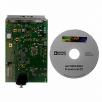
Manufacturer Part Number
EVAL-AD7766-1EDZ
Description
BOARD EVAL AD7766-1 64KSPS 111DB
Manufacturer
Analog Devices Inc
Specifications of EVAL-AD7766-1EDZ
Number Of Adc's
1
Number Of Bits
24
Sampling Rate (per Second)
64k
Data Interface
Serial
Inputs Per Adc
1 Differential
Input Range
±VREF
Power (typ) @ Conditions
10.5mW @ 64kSPS
Voltage Supply Source
Analog and Digital
Operating Temperature
-40°C ~ 105°C
Utilized Ic / Part
AD7766-1
Lead Free Status / RoHS Status
Lead free / RoHS Compliant


AD7766/AD7766-1/AD77662-2 INTERFACE
The AD7766/AD7766-1/AD7766-2 provide the user with a
flexible serial interface, enabling the user to implement the
most desirable interfacing scheme for their application. Each
AD7766/AD7766-1/AD7766-2 interface comprises seven
different signals. Five of these signals are inputs: MCLK, CS ,
SYNC / PD , SCLK, and SDI. The other two signals are outputs:
DRDY and SDO.
INITIAL POWER-UP
On initial power-up, apply a continuous MCLK signal. It is recom-
mended that the user reset the AD7766/AD7766-1/AD7766-2
to clear the filters and ensure correct operation. The reset is
completed as shown in Figure 5, with all events occurring relative
to the rising edge of MCLK. A negative pulse on the SYNC / PD
input initiates the reset, and the DRDY output switches to logic
high and remains high until valid data is available. Following the
power-up of the AD7766/AD7766-1/AD7766-2 by transitioning
the SYNC / PD pin to logic high, a settling time is required before
valid data is output by the device. This settling time, t
is a function of the MCLK frequency and the decimation rate.
Table 7
be referenced when reviewing
Table 7. Filter Settling Time After SYNC / PD
Model
AD7766
AD7766-1
AD7766-2
1
READING DATA
The AD7766/AD7766-1/AD7766-2 output data conversion
results in an MSB-first, twos complement, 24-bit format on the
serial data output (SDO) pin. MCLK is the master clock, which
controls all the AD7766/AD7766-1/AD7766-2 conversions. The
SCLK is the serial clock input for the device. All data transfers
take place with respect to the SCLK signal.
The DRDY line is used as a status signal to indicate when the data
is available to be read from the AD7766/AD7766-1/AD7766-2.
The falling edge of DRDY indicates that a new data-word is
available in the output register of the device. DRDY stays low
during the period that output data is permitted to be read from
the SDO pin. The DRDY signal returns to logic high to indicate
when not to read from the device. Ensure that a data read is not
attempted during this period while the output register is being
updated.
t
to the falling edge of DRDY .
SETTLING
is measured from the first MCLK rising edge after the rising edge of SYNC / PD
lists the settling time of each AD7766 model and should
Decimation Rate
8
16
32
Figure 5
.
t
(594 × t
(1186 × t
(2370 × t
SETTLING
1
MCLK
MCLK
MCLK
) + t
) + t
) + t
SETTLING
21
21
21
,
Rev. C | Page 17 of 24
The AD7766/AD7766-1/AD7766-2 offer the option of using a
chip select input signal ( CS ) in a data read cycle. The CS signal is
a gate for the SDO pin and allows many AD7766/AD7766-1/
AD7766-2 devices to share the same serial bus. It acts as an
instruction signal to each of these devices indicating permission
to use the bus. When CS is logic high, the SDO line of the
AD7766/AD7766-1/AD7766-2 is tristated.
There are two distinct patterns that can be initiated to read data
from the AD7766/AD7766-1/AD7766-2 devices: a pattern for
when the CS falling edge occurs after the DRDY falling edge
and a pattern for when the CS falling edge occurs before the
DRDY falling edge (when CS is set to logic low).
When the CS falling edge occurs after the DRDY falling edge,
the MSB of the conversion result is available on the SDO line on
the CS falling edge. The remaining bits of the conversion result
(MSB − 1, MSB − 2, and so on) are clocked onto the SDO line
by the falling edges of SCLK that follow the CS falling edge.
Figure 3
When CS is tied low, the AD7766/AD7766-1/AD7766-2 serial
interfaces can operate in 3-wire mode as shown in
this case, the MSB of the conversion result is available on the
SDO line on the falling edge of
the data conversion result (MSB − 1, MSB − 2, and so on) are
clocked onto the SDO line by the subsequent SCLK falling edges.
POWER-DOWN, RESET, AND SYNCHRONIZATION
The SYNC / PD pin allows the user to synchronize multiple
AD7766/AD7766-1/AD7766-2 devices. This pin also allows the
user to reset and power down the AD7766/AD7766-1/AD7766-2
devices. These features are implemented relative to the rising edges
of MCLK and are shown in
To power down, reset, or synchronize a device, the SYNC / PD
pin should be taken low. On the first rising edge of MCLK, the
AD7766/AD7766-1/AD7766-2 are powered down. The DRDY
pin transitions to logic high, indicating that the data in the
output register is no longer valid. The status of the SYNC / PD
pin is checked on each subsequent rising edge of MCLK. On the
first rising edge of MCLK after the SYNC / PD pin is taken high,
the AD7766/AD7766-1/AD7766-2 are taken out of power-down.
On the next rising edge, the filter of the AD7766/AD7766-1/
AD7766-2 is reset. On the following rising edge, the first new
sample is taken.
A settling time, t
valid data is output by the device (see Table 7). The DRDY
output goes logic low after t
available on SDO for readback.
details this interfacing scheme.
SETTLING
, from the filter reset must elapse before
SETTLING
Figure 5
DRDY . The remaining bits of
to indicate when valid data is
, marked as A, B, C, and D.
Figure 4
AD7766
. In
Related parts for EVAL-AD7766-1EDZ
Image
Part Number
Description
Manufacturer
Datasheet
Request
R

Part Number:
Description:
IC, ADJ LDO REG, 1.5V TO 5V 250mA MSOP-8
Manufacturer:
Vishay
Datasheet:

Part Number:
Description:
IC, ADJ LDO REG, 1.5V TO 5V 0.6A 8-TSSOP
Manufacturer:
Vishay
Datasheet:
Part Number:
Description:
IC, ADJ LDO REG, 1.5V TO 5V 250mA MSOP-8
Manufacturer:
Vishay
Datasheet:

Part Number:
Description:
IC ADJ LDO REG 1.5V TO 5V 150mA 5-SOT-23
Manufacturer:
Vishay
Datasheet:

Part Number:
Description:
BOARD EVAL AS1324-AD
Manufacturer:
austriamicrosystems
Datasheet:
Part Number:
Description:
IC, ADJ LDO REG, 1.5V TO 5V 0.6A 8-TSSOP
Manufacturer:
Vishay
Datasheet:

Part Number:
Description:
IC, ADJ LDO REG, 1.5V TO 5V, 0.3A, MSOP8
Manufacturer:
Vishay
Datasheet:
Part Number:
Description:
IC, ADJ LDO REG, 1.5V TO 5V, 0.3A, MSOP8
Manufacturer:
Vishay
Datasheet:
Part Number:
Description:
IC, ADJ LDO REG 1.215V TO 5V 0.3A MSOP-8
Manufacturer:
Vishay
Datasheet:
Part Number:
Description:
IC, ADJ LDO REG 1.215V TO 5V 0.3A MSOP-8
Manufacturer:
Vishay
Datasheet:

Part Number:
Description:
±1.7g Dual-Axis IMEMS Accelerometer Evaluation Board
Manufacturer:
Analog Devices Inc
Datasheet:

Part Number:
Description:
IC MULTIPLIER ANALOG 8-SOIC T/R
Manufacturer:
Analog Devices Inc
Datasheet:

Part Number:
Description:
IC ANALOG MULTIPLIER 8-DIP
Manufacturer:
Analog Devices Inc
Datasheet:
Part Number:
Description:
IC ANALOG MULTIPLIER 8-SOIC
Manufacturer:
Analog Devices Inc
Datasheet:
Part Number:
Description:
IC ANALOG MULTIPLIER 8-DIP
Manufacturer:
Analog Devices Inc
Datasheet: