SSM2306-MINI-EVALZ Analog Devices Inc, SSM2306-MINI-EVALZ Datasheet - Page 4
SSM2306-MINI-EVALZ
Manufacturer Part Number
SSM2306-MINI-EVALZ
Description
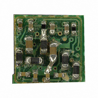
BOARD EVAL FOR SSM2306-MINI
Manufacturer
Analog Devices Inc
Specifications of SSM2306-MINI-EVALZ
Design Resources
Analog Audio Input, Class-D Output with ADAU1701, SSM2306, and ADP3336 (CN0162)
Amplifier Type
Class D
Output Type
2-Channel (Stereo)
Max Output Power X Channels @ Load
2.4W x 2 @ 4 Ohm
Voltage - Supply
2.5 V ~ 5 V
Operating Temperature
-40°C ~ 85°C
Board Type
Fully Populated
Utilized Ic / Part
SSM2306
Lead Free Status / RoHS Status
Lead free / RoHS Compliant


EVAL-SSM2306-MINI
PCB LAYOUT GUIDELINES
Correct PCB layout is critical in application designs to prevent
EMI from exceeding allowable limits and to ensure that the
amplifier chip operates below the temperature limit. Follow
these guidelines carefully when designing the PCB layout.
1.
2.
3.
4.
5.
6.
Place nine vias onto the thermal pad of the amplifier. The
outer diameter of the vias should be 0.5 mm, and the inner
diameter should be 0.33 mm. Use a PCB area of at least
2 cm
layer as the heat sink (see Figure 4 and Figure 5). If internal
layers are available in the PCB, allocate an area as large as
possible to the ground planes and connect these vias to the
ground planes.
Place the EMI filtering beads (B1, B2, B3, and B4) as close
to the amplifier chip as possible.
Place the decoupling capacitors for the beads (C5, C6, C7,
and C8) as close to the amplifier chip as possible, and
connect all their ground terminals together.
Place the first decoupling capacitor for the power supply
(C9) as close to the amplifier chip as possible, and connect
its ground terminal directly to the IC GND pins (Pin 13
and Pin 16).
Place the other decoupling capacitor for the power supply
(C10) as close to the amplifier chip as possible, and connect
its ground terminal to the PCB ground area from which
the power supply traces come.
Place the bead for the power supply (B5) as close to the
amplifier chip as possible, and keep it on the same side of
the PCB as the chip.
2
or an equivalent area on the back side of the PCB
Rev. 0 | Page 4 of 8
7.
8.
9.
10. Use a solid polygon plane on the other side of the PCB for
11. Keep the PCB traces of high EMI nodes on the same side of
The SSM2306 mini evaluation board works well only if these
techniques are implemented in the PCB design to keep EMI and
amplifier temperature low.
The ferrite beads can block EMI up to 160 MHz. To
eliminate EMI higher than 160 MHz, place a low value,
small size capacitor, such as a 100 pF, 0402 size capacitor,
in parallel with the decoupling capacitors, C5, C6, C7, and
C8. Place this small capacitor at least 20 mm away from the
1 nF decoupling capacitor. Ideally, the ground terminals of
these small capacitors should be connected to the ground
terminals of the 1 nF decoupling capacitors or to the PCB
traces, which are placed as close to the output loads (the
loudspeakers) as possible. In this way, the PCB connecting
trace between these two capacitors serves as an inductor
for filtering out the high frequency component.
Ground the unconnected pins, Pin 6 and Pin 7.
Connect the GND pins, Pin 13 and Pin 16, to the thermal
pad and place grounding vias, as shown in Figure 3 and
Figure 4.
the area of the vias that are placed on the thermal pad of
the chip. See Figure 4 or Figure 5. This polygon serves as
both the EMI shielding ground plane and the heat sink for
the SSM2306.
the PCB and as short as possible. The high EMI nodes on
the SSM2306 are Pin 1, Pin 2, Pin 11, and Pin 12.
Related parts for SSM2306-MINI-EVALZ
Image
Part Number
Description
Manufacturer
Datasheet
Request
R

Part Number:
Description:
BOARD EVAL FOR SSM2306
Manufacturer:
Analog Devices Inc
Datasheet:

Part Number:
Description:
2 W, Filterless, Class-D Stereo Audio Amplifier
Manufacturer:
AD [Analog Devices]
Datasheet:

Part Number:
Description:
±1.7g Dual-Axis IMEMS Accelerometer Evaluation Board
Manufacturer:
Analog Devices Inc
Datasheet:

Part Number:
Description:
Inertial Sensor Evaluation System
Manufacturer:
Analog Devices Inc
Datasheet:
Part Number:
Description:
Manufacturer:
Analog Devices Inc
Datasheet:
Part Number:
Description:
Manufacturer:
Analog Devices Inc
Datasheet:
Part Number:
Description:
Manufacturer:
Analog Devices Inc
Datasheet:
Part Number:
Description:
Manufacturer:
Analog Devices Inc
Datasheet:
Part Number:
Description:
Manufacturer:
Analog Devices Inc
Datasheet:
Part Number:
Description:
Manufacturer:
Analog Devices Inc
Datasheet:
Part Number:
Description:
Manufacturer:
Analog Devices Inc
Datasheet:
Part Number:
Description:
Manufacturer:
Analog Devices Inc
Datasheet:
Part Number:
Description:
Manufacturer:
Analog Devices Inc
Datasheet: