MCP1630DM-DDBS2 Microchip Technology, MCP1630DM-DDBS2 Datasheet - Page 13
MCP1630DM-DDBS2
Manufacturer Part Number
MCP1630DM-DDBS2
Description
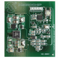
BOARD DEMO BOOST COUPLED INDUCTR
Manufacturer
Microchip Technology
Type
DC/DC Switching Converters, Regulators & Controllersr
Specifications of MCP1630DM-DDBS2
Main Purpose
DC/DC, Step Up
Outputs And Type
1, Non-Isolated
Voltage - Output
15 ~ 40V
Current - Output
30mA
Voltage - Input
3 ~ 5.5V
Regulator Topology
Boost
Frequency - Switching
100kHz
Board Type
Fully Populated
Utilized Ic / Part
MCP1630
Output Voltage
15 V to 40 V
Product
Power Management Modules
For Use With/related Products
MCP1630, PIC12F683
Lead Free Status / RoHS Status
Not applicable / Not applicable
Power - Output
-
Lead Free Status / Rohs Status
Lead free / RoHS Compliant


©
2006 Microchip Technology Inc.
2.3.1.2
A variable resistive load can be used to verify the line and load regulation. The load
resistance is connected between the TP3 and TP4 test points. To measure the output
voltage, connect the common lead of the multi meter to TP4 and the positive terminal
to TP3. By varying the load, the load regulation can be verified by measuring the output
voltage over the entire load range of 0 mA to 30 mA. Similarly, by varying the line
voltage from 3V to 5.5V and checking the output voltage, the line regulation can be
calculated.
Evaluating the Application
The best way to evaluate the MCP1630 Coupled Inductor Boost Converter Demo
Board is to dig into the circuit. Measure voltages and currents with a Digital Volt Meter
(DVM) and probe the board with an oscilloscope.
The voltage on the switching node can be calculated below.
Firmware
The PIC12F683 device comes preprogrammed with firmware to operate the system as
described above. The firmware flow diagram is shown in Appendix C. “Demo Board
Firmware”.
The program is fairly simple and straight forward. There is an initialization routine at the
beginning of the program.
The internal oscillator clock is set to 8 MHz.The TRISIO is configured to set GP2
(Oscillator pulses to the MCP1630) and GP5 (V
port and GP3 (Push button S1) as Input Port.The OPTION register is configured to
wake-up on Port pin change of GP3.
The TMR0 is initialized with a value which causes TMR0 to overflow after 10 ms The
TMR0 overflow interrupt is also enabled. Initialize registers TEMP and TEMP2 for 2
seconds time measurement.
The PWM duty cycle is specified by writing to the CCPR1L register and to the
CCP1CON <5:4> bits. The CCPR1L contains the eight MSbs and the CCP1CON <5:4>
contains the two LSbs. This 10-bit value is represented by CCPR1L:CCP1CON <5:4>.
The switching frequency is set to 100 kHz.
Where:
TMR0 overflow occurs for every 10 ms.
TEMP and TEMP2 counts for 2 seconds (TEMP2 = 10, TEMP = 20)
Hence 10 * 20 * 10 ms = 2 Seconds)
N
APPLYING LOAD TO MCP1630 COUPLED INDUCTOR BOOST
CONVERTER DEMO BOARD
1
V
& N
V
OUT
V
SW
V
IN
D
2
= Voltage across switch
= Output Voltage
= Diode Drop
= Input Voltage
= Coupled Inductor Turns Ratio
(N
V
SW
1
and N
=
V
IN
2
is 1 for a 1:1 ratio coupled inductor)
+
(
V
OUT
+
V
D
REF
–
V
Voltage to MCP1630) as an output
IN
)
------------------- -
N
1
N
+
2
N
2
DS51612A-page 9
Related parts for MCP1630DM-DDBS2
Image
Part Number
Description
Manufacturer
Datasheet
Request
R

Part Number:
Description:
BOARD DEMO BOOST AUTO INPUT
Manufacturer:
Microchip Technology
Datasheet:

Part Number:
Description:
BOARD CONV DEMO MCP1630 TRPL-OUT
Manufacturer:
Microchip Technology
Datasheet:

Part Number:
Description:
BOARD DEMO FOR MCP1630
Manufacturer:
Microchip Technology
Datasheet:

Part Number:
Description:
BOARD DEMO MCP1630 BIAS SUPPLY
Manufacturer:
Microchip Technology
Datasheet:

Part Number:
Description:
BOARD DEM MCP1630 BOOST MODE LED
Manufacturer:
Microchip Technology
Datasheet:

Part Number:
Description:
Manufacturer:
Microchip Technology Inc.
Datasheet:
Part Number:
Description:
Manufacturer:
Microchip Technology Inc.
Datasheet:
Part Number:
Description:
Manufacturer:
Microchip Technology Inc.
Datasheet:
Part Number:
Description:
Manufacturer:
Microchip Technology Inc.
Datasheet:
Part Number:
Description:
Manufacturer:
Microchip Technology Inc.
Datasheet:
Part Number:
Description:
Manufacturer:
Microchip Technology Inc.
Datasheet: