MCP1630DM-DDBS2 Microchip Technology, MCP1630DM-DDBS2 Datasheet - Page 14
MCP1630DM-DDBS2
Manufacturer Part Number
MCP1630DM-DDBS2
Description
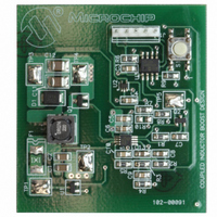
BOARD DEMO BOOST COUPLED INDUCTR
Manufacturer
Microchip Technology
Type
DC/DC Switching Converters, Regulators & Controllersr
Specifications of MCP1630DM-DDBS2
Main Purpose
DC/DC, Step Up
Outputs And Type
1, Non-Isolated
Voltage - Output
15 ~ 40V
Current - Output
30mA
Voltage - Input
3 ~ 5.5V
Regulator Topology
Boost
Frequency - Switching
100kHz
Board Type
Fully Populated
Utilized Ic / Part
MCP1630
Output Voltage
15 V to 40 V
Product
Power Management Modules
For Use With/related Products
MCP1630, PIC12F683
Lead Free Status / RoHS Status
Not applicable / Not applicable
Power - Output
-
Lead Free Status / Rohs Status
Lead free / RoHS Compliant


MCP1630 Coupled Inductor Boost Converter Demo Board User’s Guide
DS51612A-page 10
Upon powering on, the processor enters into SLEEP mode after the ports are initialized
and registers configured. The processor wakes-up from SLEEP mode if the push
button S1 on GP3 is pressed. TEMP and TEMP2 registers check weather the push
button S1 is pressed for more than 2 seconds. If the push button S1 is pressed for less
than 2 seconds, will not allow the TEMP1 register to set, which indicates that the push
button is not pressed for more than 2 seconds and the processor goes back to SLEEP
mode.
Once the processor is on after the push button is pressed for 2 seconds, the output
voltage is set at 40V by generating V
V
Voltages.
Period is fixed for 508 µs ~= 1.94 kHz.
Off Time (Duty cycle) is varied from 308 µs to 508 µs.
Each short depression of push button S1 will load different duty cycles to generate
different V
reducing steps of 5V in cyclic order. A key debounce delay of 300 ms is introduced
between each short push button depressions.
At any of the output voltages, if the push button S1 is pressed for more than 2 seconds,
the processor goes into SLEEP mode by clearing the TEMP1 register.
Again, a subsequent depression of push button S1 for more than 2 seconds wakes the
processor form SLEEP mode by setting the TEMP1 register and output is powered at
40V.
The firmware program in the PIC12F683 device can be edited to modify the operation
of the application.
An additional feature can be incorporated in the firmware program where one can vary
the output voltage depending on the board ambient temperature. The MCP9700 Linear
Active Thermistor provided on-board can be directly interfaced to a MCU, and the
firmware suitably modified to achieve the objective.This feature is presently not
implemented in this demo board.
Programming
Header J1 is provided for in-circuit programming. This is an optional feature, since the
MCP1630 Coupled Inductor Boost Converter Demo Board comes preprogrammed with
firmware to operate the system. The PIC12F683 device can be reprogrammed with the
Baseline Flash Microcontroller Programmer (BFMP).
REF
Off time @ Duty Cycle
Voltage. The duty cycle and period values are loaded to generate different V
REF
voltages which decrements the output voltage from 40V to 15V in
=
=
=
=
=
=
00 is 00 µs (For 40V Output)
10 is 64 µs (For 35V Output)
20 is 128 µs (For 30V Output)
30 is 192 µs (For 25V Output)
40 is 256 µs (For 20V Output)
50 is 320 µs (For 15V Output)
REF
Voltage. TMR1 is configured for generating
©
2006 Microchip Technology Inc.
REF
Related parts for MCP1630DM-DDBS2
Image
Part Number
Description
Manufacturer
Datasheet
Request
R

Part Number:
Description:
BOARD DEMO BOOST AUTO INPUT
Manufacturer:
Microchip Technology
Datasheet:

Part Number:
Description:
BOARD CONV DEMO MCP1630 TRPL-OUT
Manufacturer:
Microchip Technology
Datasheet:

Part Number:
Description:
BOARD DEMO FOR MCP1630
Manufacturer:
Microchip Technology
Datasheet:

Part Number:
Description:
BOARD DEMO MCP1630 BIAS SUPPLY
Manufacturer:
Microchip Technology
Datasheet:

Part Number:
Description:
BOARD DEM MCP1630 BOOST MODE LED
Manufacturer:
Microchip Technology
Datasheet:

Part Number:
Description:
Manufacturer:
Microchip Technology Inc.
Datasheet:
Part Number:
Description:
Manufacturer:
Microchip Technology Inc.
Datasheet:
Part Number:
Description:
Manufacturer:
Microchip Technology Inc.
Datasheet:
Part Number:
Description:
Manufacturer:
Microchip Technology Inc.
Datasheet:
Part Number:
Description:
Manufacturer:
Microchip Technology Inc.
Datasheet:
Part Number:
Description:
Manufacturer:
Microchip Technology Inc.
Datasheet: