DM300023 Microchip Technology, DM300023 Datasheet - Page 5
DM300023
Manufacturer Part Number
DM300023
Description
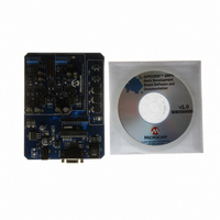
KIT DEMO DSPICDEM SMPS BUCK
Manufacturer
Microchip Technology
Series
dsPIC™r
Datasheets
1.AC164335.pdf
(286 pages)
2.DM300023.pdf
(22 pages)
3.DM300023.pdf
(18 pages)
4.DM300023.pdf
(50 pages)
5.DM300023.pdf
(16 pages)
Specifications of DM300023
Main Purpose
DC/DC, Step Down
Outputs And Type
2, Non-Isolated
Voltage - Input
7 ~ 15V
Regulator Topology
Buck
Board Type
Fully Populated
Utilized Ic / Part
dsPIC30F2020
Processor To Be Evaluated
dsPIC30F202x/1010
Interface Type
RS-232
Lead Free Status / RoHS Status
Lead free / RoHS Compliant
Current - Output
-
Voltage - Output
-
Power - Output
-
Frequency - Switching
-
Lead Free Status / Rohs Status
Lead free / RoHS Compliant
Available stocks
Company
Part Number
Manufacturer
Quantity
Price
Company:

Part Number:
DM300023
Manufacturer:
Microchip Technology
Quantity:
135
Company:
Part Number:
DM300023
Manufacturer:
MICROCHIP
Quantity:
12 000


5. Module: PWM Duty Cycle
EQUATION 1:
© 2008 Microchip Technology Inc.
The Power Supply PWM module has a feature to
enable immediate duty cycle updates. This feature
is enabled by setting IUE = 1 in the PWMCONx
register. The dsPIC30F1010/202X Device Data
Sheet states that the minimum PWM duty cycle
value is 0x0010. Duty cycle values less than
0x0010 should cause the PWM outputs to display
states corresponding to a duty cycle value of
0x0000.
When the immediate duty cycle updates are
enabled, and a value of 0x0010 or less is loaded
into the selected duty cycle register, the outputs of
the PWM generator (PWMxH and PWMxL) will
exhibit a state opposite to the expected state. For
example, if the expected state of the PWM output
is a continuous ‘0’, then a continuous ‘1’ will be
observed, and vice versa.
The above behavior applies when the Master Duty
Cycle (MDC register) or Individual Duty Cycle
(PDCx register) provides the duty cycle value.
Work around
If immediate duty cycle updates are enabled, do
not load the duty cycle register with a value less
than or equal to 0x0010. If immediate duty cycle
updates are not enabled, no action is required
because the correct PWM state will be exhibited
for all duty cycle values.
PWMxH = (OVRDAT<1>) AND (CLDAT<1>) AND (FLTDAT<1>) = 0 AND 0 AND 1 = 0
PWMxL = (OVRDAT<0>) AND (CLDAT<0>) AND (FLTDAT<0>) = 0 AND 1 AND 0 = 0
6. Module: PWM Override Priority
dsPIC30F1010/202X
The “dsPIC30F1010/202X Family Data Sheet”
(DS70178) states the priority of PWMx pin
ownership as:
• PWM Generator (lowest priority)
• Output Override
• Current-Limit Override
• Fault Override
• PENx (GPIO/PWM) ownership (highest priority)
Instead of following the above priority scheme, the
PWMx pin ownership is determined by ANDing the
Output Override Data bits (OVRDAT<1:0>),
Current-Limit Override Data bits (CLDAT<1:0>),
and Fault Override Data bits (FLTDAT<1:0>) in the
IOCONx register.
For example, the override data may be set as
follows:
• OVRDAT<1:0> = 00
• CLDAT<1:0> = 01
• FLTDAT<1:0> = 10
If all three overrides occur simultaneously, the
following operations shown in Equation 1 will
determine the state of the PWMx pin.
Therefore,
simultaneously, only the override data for the
active override sources will be ANDed together
while the inactive override sources will be ignored.
If only one override is active, override priorities do
not apply and operation of the PWM overrides is
normal.
Work around
None.
when
multiple
overrides
DS80319D-page 5
occur
Related parts for DM300023
Image
Part Number
Description
Manufacturer
Datasheet
Request
R

Part Number:
Description:
Manufacturer:
Microchip Technology Inc.
Datasheet:
Part Number:
Description:
Manufacturer:
Microchip Technology Inc.
Datasheet:
Part Number:
Description:
Manufacturer:
Microchip Technology Inc.
Datasheet:
Part Number:
Description:
Manufacturer:
Microchip Technology Inc.
Datasheet:
Part Number:
Description:
Manufacturer:
Microchip Technology Inc.
Datasheet:
Part Number:
Description:
Manufacturer:
Microchip Technology Inc.
Datasheet:
Part Number:
Description:
Manufacturer:
Microchip Technology Inc.
Datasheet:
Part Number:
Description:
Manufacturer:
Microchip Technology Inc.
Datasheet: