DM300023 Microchip Technology, DM300023 Datasheet - Page 6
DM300023
Manufacturer Part Number
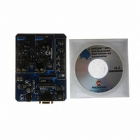
DM300023
Description
KIT DEMO DSPICDEM SMPS BUCK
Manufacturer
Microchip Technology
Series
dsPIC™r
Datasheets
1.AC164335.pdf
(286 pages)
2.DM300023.pdf
(22 pages)
3.DM300023.pdf
(18 pages)
4.DM300023.pdf
(50 pages)
5.DM300023.pdf
(16 pages)
Specifications of DM300023
Main Purpose
DC/DC, Step Down
Outputs And Type
2, Non-Isolated
Voltage - Input
7 ~ 15V
Regulator Topology
Buck
Board Type
Fully Populated
Utilized Ic / Part
dsPIC30F2020
Processor To Be Evaluated
dsPIC30F202x/1010
Interface Type
RS-232
Lead Free Status / RoHS Status
Lead free / RoHS Compliant
Current - Output
-
Voltage - Output
-
Power - Output
-
Frequency - Switching
-
Lead Free Status / Rohs Status
Lead free / RoHS Compliant
Available stocks
Company
Part Number
Manufacturer
Quantity
Price
Company:

Part Number:
DM300023
Manufacturer:
Microchip Technology
Quantity:
135
Company:
Part Number:
DM300023
Manufacturer:
MICROCHIP
Quantity:
12 000


dsPIC30F1010/202X
7. Module: PWM Jitter
TABLE 1:
EQUATION 2:
EQUATION 3:
DS80319D-page 6
Speed of Operation
The outputs of the PWM module may exhibit a
jitter proportional to the speed of operation of the
device. The jitter may be observed as a deviation
in the PWM Period, Duty Cycle or Phase, and may
be affected independent of each other. As a result,
the maximum deviation exhibited on the PWM
output pin at 30 MIPS is 8.4 nsec.
The jitter is caused by silicon process variations,
noise on the V
temperature of the dsPIC DSC. However, for a
given set of operating conditions, the maximum
jitter will be the same for all three parameters, and
independent of each other.
Table 1 shows the maximum jitter that may be
exhibited at various operating speeds.
The maximum jitter at any operating speed can be
determined using Equation 2.
Where:
• S is the speed of operation in MIPS.
The maximum percentage error observed on the
PWM output can be calculated using Equation 3.
Where:
• x
• x
Work around
Operate the Power Supply PWM module so that
the percentage error in the parameter of interest
(from Equation 3) is within permissible limits of the
application.
Error (%)
Maximum jitter observed (nsec)
interest (PWM period, Duty Cycle or Phase).
parameter of interest (PWM period, Duty Cycle
or Phase).
observed
programmed
30 MIPS
20 MIPS
15 MIPS
=
is the observed value of parameter of
±
is the programmed value of
(
-------------------------------------------------------------- -
x
programmed
DD
x
programmed
rail and the operating
Maximum Jitter on
–
PWM Output
x
observed
12.6 nsec
16.8 nsec
8.4 nsec
=
252
-------- -
S ( )
)
⋅
100
8. Module: ADC Module: Global Software
In order to perform multiple analog-to-digital
conversions using the global software trigger, the
PxRDY bits in the ADSTAT register must be
cleared. The data sheet indicates that the user can
configure the ADC pin pairs to perform a
conversion when the GSWTRG bit in the ADCON
register is set. When the conversion is available,
the user must then clear the GSWTRG bit and set
it again to perform another conversion. Contrary to
what the data sheet indicates, this will not initiate
another conversion unless the PxRDY bits are
cleared. Clearing the PxRDY bits automatically
clears the GSWTRG bit.
This only applies to a polling based approach. If an
interrupt based approach is used, the user is
required to clear the PxRDY bits in the ADC
Interrupt Service Routine (ISR).
Work around
The following sequence should be followed to
manually trigger ADC conversions using the
global software trigger (polling based only.)
1. Set the GSWTRG bit in ADCON to initiate a
2. Check the PxRDY bits to determine when the
3. Clear the PxRDY bits. The GSWTRG bit will be
4. Repeat steps 1 to 3 to perform additional
Alternatively, the individual software trigger can be
selected by setting the TRGSRCx<5:0> bits in the
ADCPCx register equal to 0x01. Instead of using
the global software trigger, the individual software
trigger (ADCPCx<SWTRGx>) bits can be used to
trigger a conversion on a given analog pin pair. In
a bit polling approach, the PENDx in the ADCPCx
register should be used to determine when a
conversion is completed. In an interrupt based
approach, the PxRDY bits get set when the
conversion is complete. This bit must be cleared in
the ADC Interrupt Service Routine in order to
enable future interrupts.
conversion on channels which have the trigger
source as the global software trigger (via the
TRGSRCx<5:0> bits in the ADCPCx
registers).
conversion(s) is completed.
cleared as a result of this operation.
conversions.
Trigger
© 2008 Microchip Technology Inc.
Related parts for DM300023
Image
Part Number
Description
Manufacturer
Datasheet
Request
R

Part Number:
Description:
Manufacturer:
Microchip Technology Inc.
Datasheet:
Part Number:
Description:
Manufacturer:
Microchip Technology Inc.
Datasheet:
Part Number:
Description:
Manufacturer:
Microchip Technology Inc.
Datasheet:
Part Number:
Description:
Manufacturer:
Microchip Technology Inc.
Datasheet:
Part Number:
Description:
Manufacturer:
Microchip Technology Inc.
Datasheet:
Part Number:
Description:
Manufacturer:
Microchip Technology Inc.
Datasheet:
Part Number:
Description:
Manufacturer:
Microchip Technology Inc.
Datasheet:
Part Number:
Description:
Manufacturer:
Microchip Technology Inc.
Datasheet: