STEVAL-ISA052V1 STMicroelectronics, STEVAL-ISA052V1 Datasheet - Page 44
STEVAL-ISA052V1
Manufacturer Part Number
STEVAL-ISA052V1
Description
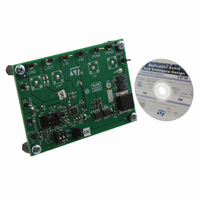
KIT EVAL PM6675S HE CTLR 2A REG
Manufacturer
STMicroelectronics
Specifications of STEVAL-ISA052V1
Main Purpose
DC/DC, Step Down with LDO
Outputs And Type
2, Non-Isolated
Voltage - Output
1.5V, 0.6 ~ 3.3V
Current - Output
10A, 2A
Voltage - Input
4.5 ~ 28 V
Regulator Topology
Buck
Board Type
Fully Populated
Utilized Ic / Part
PM6675
Product
Power Management Modules
Lead Free Status / RoHS Status
Lead free / RoHS Compliant
Power - Output
-
Frequency - Switching
-
Lead Free Status / Rohs Status
Lead free / RoHS Compliant
Other names
497-8426
Available stocks
Company
Part Number
Manufacturer
Quantity
Price
Company:

Part Number:
STEVAL-ISA052V1
Manufacturer:
STMicroelectronics
Quantity:
1


Application information
44/53
where R
Switching losses are approximately given by:
Equation 42
where t
gate-driver current capability and the gate charge Q
low R
As general rule, the R
MOSFET.
Logic-level MOSFETs are recommended, as long as low-side and high-side gate drivers are
powered by V
greater than the maximum input voltage V
Below some tested high-side MOSFETs are listed.
Table 14.
In buck converters the power dissipation of the synchronous MOSFET is mainly due to
conduction losses:
Equation 43
Maximum conduction losses occur at the maximum input voltage:
Equation 44
The synchronous rectifier should have the lowest R
MOSFET turns on, high d
through its gate-drain capacitance C
the choice of the low-side MOSFET is a trade-off between on resistance and gate charge; a
good selection should minimizes the ratio C
Equation 45
Below some tested low-side MOSFETs are listed.
Manufacturer
DSon
ON
P
DS(on)
ST
IR
switching
. Unfortunately low R
and t
Evaluated high-side MOSFETs
VCC
is the drain-source on-resistance of the control MOSFET.
OFF
=
= +5 V. The breakdown voltage of the MOSFETs (V
V
are the turn-on and turn-off times of the MOSFET and depend on the
IN
DS(on)
STS12NH3LL
⋅
I (
IRF7811
P
LOAD
V
Type
conduction
/d
x Q
t
(max)
of the phase node can bring up even the low-side gate
DSon
gate
2
=
−
P
product should be minimized to find the suitable
R
RRS
MOSFETs have a great gate charge.
C
DLowSide
∆
DSon
2
GS
I
L
, causing a cross-conduction problem. Once again,
)
R
=
⋅
INmax
(mΩ)
⋅
t
DS(on)
10.5
⎛
⎜
⎜
⎝
C
on
9
RSS
1
≅
ISS
−
⋅
P
f
.
sw
V
conduction
−
V
/ C
IN
OUT
C
+
,
MAX
gate
DS(on)
GS
RSS
V
IN
. A greater efficiency is achieved with
where
⎞
⎟
⎟
⎠
⋅
⋅
I (
Gate charge
I
LOAD
as possible. When the high-side
LOAD
(nC)
12
18
,
MAX
(max)
2
2
+
BRDSS
∆
2
I
L
)
⋅
Rated reverse
t
) must be
off
voltage (V)
⋅
f
sw
30
30
PM6675S
Related parts for STEVAL-ISA052V1
Image
Part Number
Description
Manufacturer
Datasheet
Request
R

Part Number:
Description:
BOARD RGB CTR ST7,STP08C596MTR
Manufacturer:
STMicroelectronics
Datasheet:

Part Number:
Description:
Power Management IC Development Tools Full Speed USB to RS232 Bridge Demo
Manufacturer:
STMicroelectronics
Datasheet:
Part Number:
Description:
Power Management IC Development Tools 2.5W solar eval BRD USB SPV1040 LD39050
Manufacturer:
STMicroelectronics
Datasheet:

Part Number:
Description:
BOARD EVAL FOR MEMS SENSORS
Manufacturer:
STMicroelectronics
Datasheet:

Part Number:
Description:
KIT DEV STARTER ST10F276Z5
Manufacturer:
STMicroelectronics
Datasheet:

Part Number:
Description:
BOARD EVAL HDMI $ VIDEO SWITCH
Manufacturer:
STMicroelectronics
Datasheet:

Part Number:
Description:
BOARD DEMO ACCELEROMETER DIL24
Manufacturer:
STMicroelectronics
Datasheet:

Part Number:
Description:
BOARD STLM75/STDS75/ST72F651
Manufacturer:
STMicroelectronics
Datasheet:

Part Number:
Description:
EVAL BOARD 3AXIS MEMS ACCELLRMTR
Manufacturer:
STMicroelectronics
Datasheet:

Part Number:
Description:
BOARD EVAL 8BIT MICRO + TDE1708
Manufacturer:
STMicroelectronics
Datasheet:
Part Number:
Description:
STMicroelectronics [RIPPLE-CARRY BINARY COUNTER/DIVIDERS]
Manufacturer:
STMicroelectronics
Datasheet:
Part Number:
Description:
STMicroelectronics [LIQUID-CRYSTAL DISPLAY DRIVERS]
Manufacturer:
STMicroelectronics
Datasheet:
Part Number:
Description:
BOARD EVAL FOR MEMS SENSORS
Manufacturer:
STMicroelectronics
Datasheet: