NCP1271ADAPGEVB ON Semiconductor, NCP1271ADAPGEVB Datasheet - Page 2
NCP1271ADAPGEVB
Manufacturer Part Number
NCP1271ADAPGEVB
Description
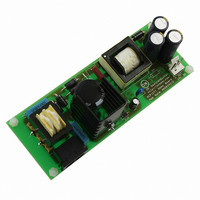
EVAL BOARD FOR NCP1271ADAPG
Manufacturer
ON Semiconductor
Datasheets
1.NCP1271P100G.pdf
(21 pages)
2.NCP1271ADAPGEVB.pdf
(1 pages)
3.NCP1271ADAPGEVB.pdf
(10 pages)
Specifications of NCP1271ADAPGEVB
Design Resources
NCP1271 Adapter EVB BOM NCP1271ADAPGEVB Gerber Files NCP1271EVB Schematic
Main Purpose
AC/DC, Primary Side
Outputs And Type
1, Isolated
Voltage - Output
19V
Current - Output
3A
Voltage - Input
85 ~ 265VAC
Regulator Topology
Flyback
Frequency - Switching
65kHz
Board Type
Fully Populated
Utilized Ic / Part
NCP1271
Silicon Manufacturer
On Semiconductor
Silicon Core Number
NCP1271
Kit Application Type
Power Management
Application Sub Type
PWM Controller
Peak Reflow Compatible (260 C)
No
Rohs Compliant
No
Lead Free Status / RoHS Status
Lead free / RoHS Compliant
Power - Output
-
Lead Free Status / Rohs Status
Lead free / RoHS Compliant
Other names
NCP1271ADAPGEVBOS


Design Steps
Step 1. Define the Specification
best choice here for (1) best stability and smallest inductor
(i.e., fewer leakage inductance and smaller size), (2) few
circuit components.
Step 2. Biasing the Controller
the NCP1271, the initial IC supply voltage, V
obtained by connecting this pin to the high voltage DC
source in Figure 2. In order to have extremely low standby
power consumption, the bias supply voltage, V
supplied by an external circuit that costs only one more
output from the flyback.
Table 1. Features of Power Supply Using NCP1271
HV
Rectified Input
Standby Condition
A Discontinuous Conduction Mode (DCM) flyback is the
Due to the integrated high−voltage startup pin (Pin 8) of
Input
Output
Features
Latch Protection
NCP1271
Fault Condition
Activated
Topology
V
CC
Figure 2. V
16 V
85 to 265 Vac, 50 Hz
19 Vdc, 3.0 A, Isolated
Excellent standby performance
Output overvoltage protection latch
Double Hiccup Restart
Soft−Skip Operation
CCM/DCM Flyback
CC
Operation Mode
Latched Off
Biasing Scheme
• Fixed−frequency current−mode control/inherent primary current limitation.
• Frequency jittering to soften EMI signature.
• Adjustable skip duty (the borderline duty between skip operation and normal
• Built−in soft−start.
• Output short−circuit fault detection implemented by an internal timer that allows
• Integrated high voltage startup that minimizes PCB spacing and loss.
• It offers excellent low standby power consumption.
• It offers low level of low−frequency audible noise.
• The soft−skip operation will be disabled if an abrupt transient load is applied from
• It minimizes power dissipation in fault and allows auto−recovery ability when fault
• V
• Reset needs the AC input unplugged.
CC
CC
fixed−freq PWM operation).
usage of bad coupling transformer.
standby operation.
is cleared.
, must be
CC
, can be
19V / 3A
Output
http://onsemi.com
stays above typical 5.8 V and PWM drive output remains off until circuit reset.
AND8242/D
2
NCP1271 is from (10 V min) and (20 max). An 18 V
clamping Zener is usually with "5% tolerance (i.e., 17.1 V
min., 18.9 V max.). When the circuit is in standby mode, the
main output voltage stays in high level because of no current
consumption, but the bias supply voltage goes lower
because of the consumption of the controller. Hence, the
biasing voltage cannot be too low and it is selected as
V
turn ratio between the main output and auxiliary winding
representing 19V:16V.
Step 3. Generic Flyback Calculation
(http://www.onsemi.com/pub/Collateral/NCP1271SHEET.
XLS). This section describes the details.
Step 3a. Define the Flyback Basic Parameter
rectified input voltage to supply to the circuit is required. It
is generally assumed that the rectified input voltages are
from 100 to 400 V that covers the rectified universal AC
input range.
V
Step 3b. Define the Transformer Turn Ratio
min, 85% max) and the skip duty (borderline duty between
normal operation and skip mode operation) is externally
adjustable. That is the design constraint in the transformer
CC
d
The application range of the bias supply voltage V
The calculation can be made by the excel spreadsheet in
The flyback itself is a DC−to−DC converter. An estimated
With the output voltage V
The design here is using the 65 kHz version of NCP1271.
The maximum allowable duty of the NCP1271 is (75%
= 1.0 V.
= 16 V. The 16 V bias supply voltage is made by a 6:5
Features
V
V
in(H)
in(L)
f = 65 kHz
out
= 100 V
= 400 V
= 19 V and output diode drop
CC
of
Related parts for NCP1271ADAPGEVB
Image
Part Number
Description
Manufacturer
Datasheet
Request
R

Part Number:
Description:
ON Semiconductor [VOLTAGE REGULATOR]
Manufacturer:
ON Semiconductor
Datasheet:
Part Number:
Description:
357-036-542-201 CARDEDGE 36POS DL .156 BLK LOPRO
Manufacturer:
ON Semiconductor
Datasheet:
Part Number:
Description:
357-036-542-201 CARDEDGE 36POS DL .156 BLK LOPRO
Manufacturer:
ON Semiconductor
Datasheet:
Part Number:
Description:
357-036-542-201 CARDEDGE 36POS DL .156 BLK LOPRO
Manufacturer:
ON Semiconductor
Datasheet:
Part Number:
Description:
357-036-542-201 CARDEDGE 36POS DL .156 BLK LOPRO
Manufacturer:
ON Semiconductor
Datasheet:
Part Number:
Description:
357-036-542-201 CARDEDGE 36POS DL .156 BLK LOPRO
Manufacturer:
ON Semiconductor
Datasheet:
Part Number:
Description:
357-036-542-201 CARDEDGE 36POS DL .156 BLK LOPRO
Manufacturer:
ON Semiconductor
Datasheet:
Part Number:
Description:
357-036-542-201 CARDEDGE 36POS DL .156 BLK LOPRO
Manufacturer:
ON Semiconductor
Datasheet:
Part Number:
Description:
357-036-542-201 CARDEDGE 36POS DL .156 BLK LOPRO
Manufacturer:
ON Semiconductor
Datasheet:
Part Number:
Description:
357-036-542-201 CARDEDGE 36POS DL .156 BLK LOPRO
Manufacturer:
ON Semiconductor
Datasheet:
Part Number:
Description:
357-036-542-201 CARDEDGE 36POS DL .156 BLK LOPRO
Manufacturer:
ON Semiconductor
Datasheet:
Part Number:
Description:
Manufacturer:
ON Semiconductor
Datasheet:
Part Number:
Description:
Manufacturer:
ON Semiconductor
Datasheet:
Part Number:
Description:
Manufacturer:
ON Semiconductor
Datasheet: