NCP1271ADAPGEVB ON Semiconductor, NCP1271ADAPGEVB Datasheet - Page 8
NCP1271ADAPGEVB
Manufacturer Part Number
NCP1271ADAPGEVB
Description
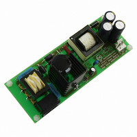
EVAL BOARD FOR NCP1271ADAPG
Manufacturer
ON Semiconductor
Datasheets
1.NCP1271P100G.pdf
(21 pages)
2.NCP1271ADAPGEVB.pdf
(1 pages)
3.NCP1271ADAPGEVB.pdf
(10 pages)
Specifications of NCP1271ADAPGEVB
Design Resources
NCP1271 Adapter EVB BOM NCP1271ADAPGEVB Gerber Files NCP1271EVB Schematic
Main Purpose
AC/DC, Primary Side
Outputs And Type
1, Isolated
Voltage - Output
19V
Current - Output
3A
Voltage - Input
85 ~ 265VAC
Regulator Topology
Flyback
Frequency - Switching
65kHz
Board Type
Fully Populated
Utilized Ic / Part
NCP1271
Silicon Manufacturer
On Semiconductor
Silicon Core Number
NCP1271
Kit Application Type
Power Management
Application Sub Type
PWM Controller
Peak Reflow Compatible (260 C)
No
Rohs Compliant
No
Lead Free Status / RoHS Status
Lead free / RoHS Compliant
Power - Output
-
Lead Free Status / Rohs Status
Lead free / RoHS Compliant
Other names
NCP1271ADAPGEVBOS


standby operation. The yellow trace is the CS pin (Pin 3)
voltage at 200 mV/div. The orange trace shows the duty that
comes from 0% to 2.27%. The figure shows that the
soft−skip time is not effectively 300 ms. In the figure, the
first five switching cycles, for about 80 ms, are in a soft−skip
period where the duty is gradually increasing. Then, the duty
follows the feedback voltage variation because the soft−skip
reference voltage is higher than the divided−by−3 feedback
voltage. It is described in Figure 34 of the data sheet.
Part II. Normal Operation
above 85%.
Part III. Dynamic Study
circuit when input is 110 Vac. Looking from the top right
side, the yellow trace is the output voltage in 5.0 V/div. The
red trace is the V
Table 2. Normal Operation Performance
Figure 11 shows a typical soft−skip pulse train during the
Table 2 shows the full load efficiency of the circuit is
Figure 12 shows the startup transient waveforms of the
120 Vac 65.4 W
180 Vac 65.2 W
220 Vac 65.2 W
230 Vac 65.2 W
265 Vac 65.2 W
110 Vac 65.4 W
85 Vac 66.4 W
Input
Figure 12. Startup Transient
CC
voltage in 5.0 V/div. The green trace is
19 V 3.0 A
19 V 3.0 A
19 V 3.0 A
19 V 3.0 A
19 V 3.0 A
19 V 3.0 A
19 V 3.0 A
Output
Efficiency
85.8%
87.2%
87.2%
87.4%
87.4%
87.4%
87.4%
http://onsemi.com
AND8242/D
8
the feedback pin voltage in 1.0 V/div. The blue trace is the
voltage across current sense resistor R8 in 500 mV/div
representing the drain current. The waveforms are captured
when V
A beginning 5.0 ms soft−start is observed in the drain
current. The green trace V
that is shorter than the 130 ms fault validation time and
hence the circuit does not enter fault condition and able to
maintain in the normal operation condition.
load operation. The output voltage does not consume current
and remains at 19 V, but the V
to 15 V because the V
current to the controller. The minimum V
transition can be 12 V. That explains why the 16 V biasing
voltage is selected and a pair of 100 mF V
needed to maintain V
order to prevent V
Conclusion
Because of the PWM controller, NCP1271, the circuit offers
low−audible−noise soft−skip mode operation, excellent
standby performance, and output overvoltage protection
latch. The design consideration of most components in the
design is explained. The design procedure is also
summarized
http://www.onsemi.com. When design with the NCP1271,
special care on (1) locate a decoupling capacitor on the
latch/skip pin (Pin 1) in order to prevent fault latchoff due to
noise and (2) locate the Vcc capacitor very close to the
controller in order to prevent entering fault condition due to
noise.
Figure 13 shows the go−to−standby transition from full
A 19 V/3.0 A flyback circuit using NCP1271 is presented.
CC
reaches V
Figure 13. Operating to Standby
in
CC
CC(on)
CC
reset.
CC
an
above V
FB
auxiliary winding still supplies
(i.e., red trace reaches 12.6 V).
drops below 3.0 V after 32 ms
CC
excel
voltage drops from 16 V
CC(off)
spreadsheet
(9.1 V typical) in
CC
CC
voltage in the
capacitor is
in
Related parts for NCP1271ADAPGEVB
Image
Part Number
Description
Manufacturer
Datasheet
Request
R

Part Number:
Description:
ON Semiconductor [VOLTAGE REGULATOR]
Manufacturer:
ON Semiconductor
Datasheet:
Part Number:
Description:
357-036-542-201 CARDEDGE 36POS DL .156 BLK LOPRO
Manufacturer:
ON Semiconductor
Datasheet:
Part Number:
Description:
357-036-542-201 CARDEDGE 36POS DL .156 BLK LOPRO
Manufacturer:
ON Semiconductor
Datasheet:
Part Number:
Description:
357-036-542-201 CARDEDGE 36POS DL .156 BLK LOPRO
Manufacturer:
ON Semiconductor
Datasheet:
Part Number:
Description:
357-036-542-201 CARDEDGE 36POS DL .156 BLK LOPRO
Manufacturer:
ON Semiconductor
Datasheet:
Part Number:
Description:
357-036-542-201 CARDEDGE 36POS DL .156 BLK LOPRO
Manufacturer:
ON Semiconductor
Datasheet:
Part Number:
Description:
357-036-542-201 CARDEDGE 36POS DL .156 BLK LOPRO
Manufacturer:
ON Semiconductor
Datasheet:
Part Number:
Description:
357-036-542-201 CARDEDGE 36POS DL .156 BLK LOPRO
Manufacturer:
ON Semiconductor
Datasheet:
Part Number:
Description:
357-036-542-201 CARDEDGE 36POS DL .156 BLK LOPRO
Manufacturer:
ON Semiconductor
Datasheet:
Part Number:
Description:
357-036-542-201 CARDEDGE 36POS DL .156 BLK LOPRO
Manufacturer:
ON Semiconductor
Datasheet:
Part Number:
Description:
357-036-542-201 CARDEDGE 36POS DL .156 BLK LOPRO
Manufacturer:
ON Semiconductor
Datasheet:
Part Number:
Description:
Manufacturer:
ON Semiconductor
Datasheet:
Part Number:
Description:
Manufacturer:
ON Semiconductor
Datasheet:
Part Number:
Description:
Manufacturer:
ON Semiconductor
Datasheet: