NCP1271ADAPGEVB ON Semiconductor, NCP1271ADAPGEVB Datasheet - Page 5
NCP1271ADAPGEVB
Manufacturer Part Number
NCP1271ADAPGEVB
Description
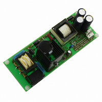
EVAL BOARD FOR NCP1271ADAPG
Manufacturer
ON Semiconductor
Datasheets
1.NCP1271P100G.pdf
(21 pages)
2.NCP1271ADAPGEVB.pdf
(1 pages)
3.NCP1271ADAPGEVB.pdf
(10 pages)
Specifications of NCP1271ADAPGEVB
Design Resources
NCP1271 Adapter EVB BOM NCP1271ADAPGEVB Gerber Files NCP1271EVB Schematic
Main Purpose
AC/DC, Primary Side
Outputs And Type
1, Isolated
Voltage - Output
19V
Current - Output
3A
Voltage - Input
85 ~ 265VAC
Regulator Topology
Flyback
Frequency - Switching
65kHz
Board Type
Fully Populated
Utilized Ic / Part
NCP1271
Silicon Manufacturer
On Semiconductor
Silicon Core Number
NCP1271
Kit Application Type
Power Management
Application Sub Type
PWM Controller
Peak Reflow Compatible (260 C)
No
Rohs Compliant
No
Lead Free Status / RoHS Status
Lead free / RoHS Compliant
Power - Output
-
Lead Free Status / Rohs Status
Lead free / RoHS Compliant
Other names
NCP1271ADAPGEVBOS


usually the bias supply voltage V
is connected to the V
18 V (±5%). In order to protect Pin 1, a 200 W is connected
to limit the current below the maximum allowed 100 mA. In
addition, an internal ESD diode will limit the maximum
voltage on Pin 1 in 10 V without damage.
output voltage is connected to a 24 V source. It can be seen
that the voltage jumps up and clamps to 10.5 V from the
nominal 1.5 V (34.8 kW × 43 mA) when the output voltage
is over 23 V typically. Once the voltage is over the 8.0 V
latch threshold, the circuit goes latch off.
Step 4b Skipping Adjustment
setting of the skip duty that the borderline duty between the
normal and skipping operation; (2) and the optimization of
the standby power consumption; (3) and indirectly increase
the latch−off immunity by lowering the Pin 1 voltage.
Due to the soft−skip mode standby operation. The
low−frequency audible noise is not a critical issue here.
Basically, the skip level (or skip duty) is set to be as high as
possible because higher value can save more power by
allowing more skipping period during standby. The
skip−level upper limit is limited by the skip duty of the
flyback, because it is not desirable to enter skip mode
operation in full load or nominal condition.
corresponds to skip duty D
below the nominal operating duty range (11.7% to 46.8% in
Step 3d) and hence the circuit does not skip in full load or
nominal condition.
Figure 5 shows how the Pin 1 voltage reacts when the
The skip resistor, R5, provides two functions: (1) the
When R5 = 34.8 kW, the skip level is R
D skip +
V skip + (R skip I skip −1.25 V) 0.73 + 0.338 V
V skip
Figure 5. Output OVP Testing
3 V
· D max + 0.338
CC
source that can be as high as
skip
= 9%. The 9% skip duty is
CC
3
. Hence, the optocoupler
· 80% + 9%
skip
= 0.338 V that
(eq. 20)
(eq. 21)
http://onsemi.com
AND8242/D
5
Step 4c. Maximum Primary Current Setting
(1) current sensing for current−mode operation; (2)and the
maximum primary current limitation. When the voltage
exceeds 1.0 V, the PWM output goes low because of
overcurrent condition. When R8 = 0.2 W, the maximum
allowable current is 5.0 A that is greater than the required
4.0 A in Step 3b.
Step 4d. Maximum Allowable Duty Setting and
Stability/Transient Response
(1) compensation ramp function in current−mode operation;
(2) and reduce the maximum duty when it is above 10 kW.
ramp in the modulation. It also means the modulation
method becomes more voltage−mode (or voltage−loop
depended) and less current−mode (or current−loop
depended). It results in slower transient response, but better
stability. If better transient response is wanted, more
current−mode modulation is needed, and the ramp resistor
value is low that makes higher loop gain. On the other hand,
if better stability is wanted, fewer current−mode modulation
is needed and the ramp resistor is high that makes slow
voltage−loop response but better stability. Figures 6 and 7
shows the transient response of the circuit recovering from
standby (output current = 0 A) to full load (output current =
3.0 A) with different values of R7. The output current is
1.0 A/div changing from 0 A to 3.0 A in green color. The
output voltages are AC−coupled, 200 mV/div, and 2.0 V/div
respectively. The input voltage is 110 Vac. It shows that the
transient response with low ramp resistor, R7, value is better.
Figures 6 and 7 also explain why the ramp resistor is below
10 kW because the transient can be bad otherwise.
Current sense resistor, R8, provides two functions:
The ramp resistor, R7, provides two functions:
Higher ramp resistor value means more compensation
Figure 6. Transient Response with R7 = 511 W
I D, max + 1 V
R CS
+ 1 V
0.2 W
+ 5 A u 4 A
(eq. 22)
Related parts for NCP1271ADAPGEVB
Image
Part Number
Description
Manufacturer
Datasheet
Request
R

Part Number:
Description:
ON Semiconductor [VOLTAGE REGULATOR]
Manufacturer:
ON Semiconductor
Datasheet:
Part Number:
Description:
357-036-542-201 CARDEDGE 36POS DL .156 BLK LOPRO
Manufacturer:
ON Semiconductor
Datasheet:
Part Number:
Description:
357-036-542-201 CARDEDGE 36POS DL .156 BLK LOPRO
Manufacturer:
ON Semiconductor
Datasheet:
Part Number:
Description:
357-036-542-201 CARDEDGE 36POS DL .156 BLK LOPRO
Manufacturer:
ON Semiconductor
Datasheet:
Part Number:
Description:
357-036-542-201 CARDEDGE 36POS DL .156 BLK LOPRO
Manufacturer:
ON Semiconductor
Datasheet:
Part Number:
Description:
357-036-542-201 CARDEDGE 36POS DL .156 BLK LOPRO
Manufacturer:
ON Semiconductor
Datasheet:
Part Number:
Description:
357-036-542-201 CARDEDGE 36POS DL .156 BLK LOPRO
Manufacturer:
ON Semiconductor
Datasheet:
Part Number:
Description:
357-036-542-201 CARDEDGE 36POS DL .156 BLK LOPRO
Manufacturer:
ON Semiconductor
Datasheet:
Part Number:
Description:
357-036-542-201 CARDEDGE 36POS DL .156 BLK LOPRO
Manufacturer:
ON Semiconductor
Datasheet:
Part Number:
Description:
357-036-542-201 CARDEDGE 36POS DL .156 BLK LOPRO
Manufacturer:
ON Semiconductor
Datasheet:
Part Number:
Description:
357-036-542-201 CARDEDGE 36POS DL .156 BLK LOPRO
Manufacturer:
ON Semiconductor
Datasheet:
Part Number:
Description:
Manufacturer:
ON Semiconductor
Datasheet:
Part Number:
Description:
Manufacturer:
ON Semiconductor
Datasheet:
Part Number:
Description:
Manufacturer:
ON Semiconductor
Datasheet: