STEVAL-ISA039V1 STMicroelectronics, STEVAL-ISA039V1 Datasheet - Page 15
STEVAL-ISA039V1
Manufacturer Part Number
STEVAL-ISA039V1
Description
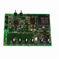
BOARD EVAL BASED ON L6727
Manufacturer
STMicroelectronics
Type
DC/DC Switching Converters, Regulators & Controllersr
Specifications of STEVAL-ISA039V1
Design Resources
STEVAL-ISA039V1 Gerber Files L6727 Eval Board Schematic STEVAL-ISA039V1 Bill of Materials
Main Purpose
DC/DC, Step Down
Outputs And Type
1, Non-Isolated
Voltage - Output
1.25V
Current - Output
5A
Voltage - Input
5 ~ 12V
Regulator Topology
Buck
Frequency - Switching
300kHz
Board Type
Fully Populated
Utilized Ic / Part
L6727
Input Voltage
5 V to 12 V
Output Voltage
1.25 V
Product
Power Management Modules
Lead Free Status / RoHS Status
Lead free / RoHS Compliant
Power - Output
-
Lead Free Status / Rohs Status
Lead free / RoHS Compliant
For Use With/related Products
L6727
Other names
497-8266
Available stocks
Company
Part Number
Manufacturer
Quantity
Price
Company:

Part Number:
STEVAL-ISA039V1
Manufacturer:
STMicroelectronics
Quantity:
1


L6727
9
9.1
9.2
Application details
Output voltage selection
L6727 is capable to precisely regulate an output voltage as low as 0.8 V. In fact, the device
comes with a fixed 0.8 V internal reference that guarantees the output regulated voltage to
be within ±1 % tolerance over line and temperature variations between 0 °C and +70 °C
(excluding output resistor divider tolerance, when present).
Output voltage higher than 0.8 V can be easily achieved by adding a resistor R
FB pin and ground. Referring to
where V
Compensation network
The control loop showed in
voltage mode type. The output voltage is regulated to the internal reference (when present,
offset resistor between FB node and GND can be neglected in control loop calculation).
Error Amplifier output is compared to oscillator saw-tooth waveform to provide PWM signal
to the driver section. PWM signal is then transferred to the switching node with V
amplitude. This waveform is filtered by the output filter.
The converter transfer function is the small signal transfer function between the output of the
EA and V
resonance and a zero at F
modulator is simply the input voltage V
ΔV
The compensation network closes the loop joining V
function ideally equal to -Z
Figure 6.
OSC
.
REF
OUT
is 0.8V.
PWM control loop
. This function has a double pole at frequency F
ΔV
OSC
ESR
F
OSC
/Z
Figure 6
V
FB
Doc ID 12933 Rev 4
OUT
depending on the output capacitor ESR. The DC Gain of the
COMPARATOR
AMPLIFIER
Figure
.
ERROR
C
F
_
+
PWM
C
P
is a voltage mode control loop. The error amplifier is a
=
R
+
_
IN
F
1, the steady state DC output voltage will be:
V
divided by the peak-to-peak oscillator voltage
REF
V
REF
Z
F
⋅
R
C
⎛
⎝
FB
S
1
V
IN
+
R
OUT
S
Z
---------- -
R
R
FB
L
OS
FB
and EA output with transfer
⎞
⎠
LC
R
C
ESR
OUT
depending on the L-C
V
Application details
OUT
OS
IN
between
OUT
15/34
Related parts for STEVAL-ISA039V1
Image
Part Number
Description
Manufacturer
Datasheet
Request
R

Part Number:
Description:
BOARD RGB CTR ST7,STP08C596MTR
Manufacturer:
STMicroelectronics
Datasheet:

Part Number:
Description:
Power Management IC Development Tools Full Speed USB to RS232 Bridge Demo
Manufacturer:
STMicroelectronics
Datasheet:
Part Number:
Description:
Power Management IC Development Tools 2.5W solar eval BRD USB SPV1040 LD39050
Manufacturer:
STMicroelectronics
Datasheet:

Part Number:
Description:
BOARD EVAL FOR MEMS SENSORS
Manufacturer:
STMicroelectronics
Datasheet:

Part Number:
Description:
KIT DEV STARTER ST10F276Z5
Manufacturer:
STMicroelectronics
Datasheet:

Part Number:
Description:
BOARD EVAL HDMI $ VIDEO SWITCH
Manufacturer:
STMicroelectronics
Datasheet:

Part Number:
Description:
BOARD DEMO ACCELEROMETER DIL24
Manufacturer:
STMicroelectronics
Datasheet:

Part Number:
Description:
BOARD STLM75/STDS75/ST72F651
Manufacturer:
STMicroelectronics
Datasheet:

Part Number:
Description:
EVAL BOARD 3AXIS MEMS ACCELLRMTR
Manufacturer:
STMicroelectronics
Datasheet:

Part Number:
Description:
BOARD EVAL 8BIT MICRO + TDE1708
Manufacturer:
STMicroelectronics
Datasheet:
Part Number:
Description:
STMicroelectronics [RIPPLE-CARRY BINARY COUNTER/DIVIDERS]
Manufacturer:
STMicroelectronics
Datasheet:
Part Number:
Description:
STMicroelectronics [LIQUID-CRYSTAL DISPLAY DRIVERS]
Manufacturer:
STMicroelectronics
Datasheet:
Part Number:
Description:
BOARD EVAL FOR MEMS SENSORS
Manufacturer:
STMicroelectronics
Datasheet: