STEVAL-ISA039V1 STMicroelectronics, STEVAL-ISA039V1 Datasheet - Page 19
STEVAL-ISA039V1
Manufacturer Part Number
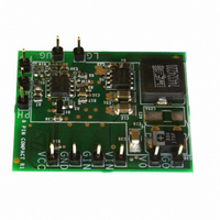
STEVAL-ISA039V1
Description
BOARD EVAL BASED ON L6727
Manufacturer
STMicroelectronics
Type
DC/DC Switching Converters, Regulators & Controllersr
Specifications of STEVAL-ISA039V1
Design Resources
STEVAL-ISA039V1 Gerber Files L6727 Eval Board Schematic STEVAL-ISA039V1 Bill of Materials
Main Purpose
DC/DC, Step Down
Outputs And Type
1, Non-Isolated
Voltage - Output
1.25V
Current - Output
5A
Voltage - Input
5 ~ 12V
Regulator Topology
Buck
Frequency - Switching
300kHz
Board Type
Fully Populated
Utilized Ic / Part
L6727
Input Voltage
5 V to 12 V
Output Voltage
1.25 V
Product
Power Management Modules
Lead Free Status / RoHS Status
Lead free / RoHS Compliant
Power - Output
-
Lead Free Status / Rohs Status
Lead free / RoHS Compliant
For Use With/related Products
L6727
Other names
497-8266
Available stocks
Company
Part Number
Manufacturer
Quantity
Price
Company:

Part Number:
STEVAL-ISA039V1
Manufacturer:
STMicroelectronics
Quantity:
1


L6727
9.4
Embedding L6727-based VRs
When embedding the VR into the application, additional care must be taken since the whole
VR is a switching DC/DC regulator and the most common system in which it has to work is a
digital system such as MB or similar. In fact, latest MBs have become faster and more
powerful: high speed data busses are more and more common and switching-induced noise
produced by the VR can affect data integrity if additional layout guidelines are not followed.
Few easy points must be considered mainly when routing traces in which switching high
currents flow (switching high currents cause voltage spikes across the stray inductance of
the traces causing noise that can affect the near traces):
When reproducing high current path on internal layers, keep all layers the same size in order
to avoid "surrounding" effects that increase noise coupling.
Keep safe guard distance between high current switching VR traces and data busses,
especially if high-speed data busses, to minimize noise coupling.
Keep safe guard distance or filter properly when routing bias traces for I/O sub-systems that
must walk near the VR.
Possible causes of noise can be located in the PHASE connections, MOSFETs gate drive
and Input voltage path (from input bulk capacitors and HS drain). Also GND connection
must be considered if not insisting on a power ground plane. These connections must be
carefully kept far away from noise-sensitive data busses.
Since the generated noise is mainly due to the switching activity of the VR, noise emissions
depend on how fast the current switches. To reduce noise emission levels, it is also possible,
in addition to the previous guidelines, to reduce the current slope and thus to increase the
switching times: this will cause, as a consequence of the higher switching time, an increase
in switching losses that must be considered in the thermal design of the system.
Doc ID 12933 Rev 4
Application details
19/34
Related parts for STEVAL-ISA039V1
Image
Part Number
Description
Manufacturer
Datasheet
Request
R

Part Number:
Description:
BOARD RGB CTR ST7,STP08C596MTR
Manufacturer:
STMicroelectronics
Datasheet:

Part Number:
Description:
Power Management IC Development Tools Full Speed USB to RS232 Bridge Demo
Manufacturer:
STMicroelectronics
Datasheet:
Part Number:
Description:
Power Management IC Development Tools 2.5W solar eval BRD USB SPV1040 LD39050
Manufacturer:
STMicroelectronics
Datasheet:

Part Number:
Description:
BOARD EVAL FOR MEMS SENSORS
Manufacturer:
STMicroelectronics
Datasheet:

Part Number:
Description:
KIT DEV STARTER ST10F276Z5
Manufacturer:
STMicroelectronics
Datasheet:

Part Number:
Description:
BOARD EVAL HDMI $ VIDEO SWITCH
Manufacturer:
STMicroelectronics
Datasheet:

Part Number:
Description:
BOARD DEMO ACCELEROMETER DIL24
Manufacturer:
STMicroelectronics
Datasheet:

Part Number:
Description:
BOARD STLM75/STDS75/ST72F651
Manufacturer:
STMicroelectronics
Datasheet:

Part Number:
Description:
EVAL BOARD 3AXIS MEMS ACCELLRMTR
Manufacturer:
STMicroelectronics
Datasheet:

Part Number:
Description:
BOARD EVAL 8BIT MICRO + TDE1708
Manufacturer:
STMicroelectronics
Datasheet:
Part Number:
Description:
STMicroelectronics [RIPPLE-CARRY BINARY COUNTER/DIVIDERS]
Manufacturer:
STMicroelectronics
Datasheet:
Part Number:
Description:
STMicroelectronics [LIQUID-CRYSTAL DISPLAY DRIVERS]
Manufacturer:
STMicroelectronics
Datasheet:
Part Number:
Description:
BOARD EVAL FOR MEMS SENSORS
Manufacturer:
STMicroelectronics
Datasheet: