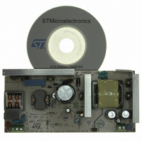
EVL6566A-75WES4 STMicroelectronics, EVL6566A-75WES4 Datasheet - Page 17

EVL6566A-75WES4
Manufacturer Part Number
EVL6566A-75WES4
Description
BOARD DEMO FOR L6563/LL6566A
Manufacturer
STMicroelectronics
Type
Power Factor Correctionr
Specifications of EVL6566A-75WES4
Main Purpose
AC/DC, Primary and Secondary Side with PFC
Outputs And Type
1, Isolated
Power - Output
75W
Voltage - Output
19V
Current - Output
4A
Voltage - Input
90 ~ 264VAC
Regulator Topology
Flyback
Board Type
Fully Populated
Utilized Ic / Part
L6563, L6566A, TSM1014
Input Voltage
90 V to 264 V
Output Voltage
19 V
Dimensions
78 mm x 170 mm
Product
Power Management Modules
Lead Free Status / RoHS Status
Lead free / RoHS Compliant
Frequency - Switching
-
Lead Free Status / Rohs Status
Lead free / RoHS Compliant
For Use With/related Products
L6563S, L6566A
Other names
497-8834
Available stocks
Company
Part Number
Manufacturer
Quantity
Price
AN2941
Figure 13. No-load operation at 90 V-60 Hz
CH1: Flyback drain
CH2: COMP pin
Standby and no-load operation
In
works in burst mode. When the feedback voltage at pin COMP falls below 2.65 V (typical),
the IC is disabled and its consumption is reduced. The chip is re-enabled as the voltage on
pin COMP rises again over this threshold. Additionally, in order to get the best efficiency,
during light-load operation the PFC stage is turned off. In fact when the voltage on pin
COMP falls below the burst mode threshold, the L6566A pin #6 (Vcc_PFC) supplying the
PFC controller, is opened. Thus the residual consumption of the PFC control circuitry is
minimized to a negligible level. Whenever the IC is shut down, either latched or not, the
Vcc_PFC pin is open as well.
In
maximum input voltage have been checked. The maximum input voltage has been chosen
because it is the most critical input voltage for transition. In fact at no load the burst pulses
have lower repetition frequency and Vcc could drop, causing restart cycles of the controller.
As visible in the graphs, both transitions are clean and there isn't any output voltage or Vcc
dip.
Figure 13
Figure 15
and
and
CH3: Output voltage
CH4: PFC drain
Figure 14
Figure 16
, some no-load waveforms are given. As shown, the L6566A
the transitions from full load to no load and vice versa at
Doc ID 15447 Rev 3
Figure 14. No-load operation at 265 V-50 Hz
CH1: Flyback Drain
CH2: COMP pin
CH3: Output voltage
CH4: PFC drain
Functional check
17/37


