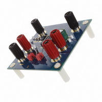
ISL8201MEVAL1Z Intersil, ISL8201MEVAL1Z Datasheet - Page 14

ISL8201MEVAL1Z
Manufacturer Part Number
ISL8201MEVAL1Z
Description
BOARD EVAL STEP-DOWN POL ISL8201
Manufacturer
Intersil
Datasheets
1.ISL8201MIRZ-T.pdf
(16 pages)
2.ISL8201MEVAL1Z.pdf
(9 pages)
3.ISL8201MEVAL1Z.pdf
(16 pages)
Specifications of ISL8201MEVAL1Z
Main Purpose
DC/DC, Step Down
Outputs And Type
1, Non-Isolated
Voltage - Output
1.5V
Current - Output
10A
Voltage - Input
1 ~ 20 V
Regulator Topology
Buck
Frequency - Switching
600kHz
Board Type
Fully Populated
Utilized Ic / Part
ISL8201
Lead Free Status / RoHS Status
Lead free / RoHS Compliant
Power - Output
-
Lead Free Status / Rohs Status
Compliant
Package Description
The structure of ISL8201M belongs to the Quad Flat-pack
No-lead package (QFN). This kind of package has
advantages, such as good thermal and electrical conductivity,
low weight and small size. The QFN package is applicable for
surface mounting technology and is being more readily used
in the industry. The ISL8201M contains several types of
devices, including resistors, capacitors, inductors and control
ICs. The ISL8201M is a copper lead-frame based package
with exposed copper thermal pads, which have good electrical
and thermal conductivity. The copper lead frame and multi
component assembly is overmolded with polymer mold
compound to protect these devices.
The package outline and typical PCB layout pattern design
and typical stencil pattern design are shown in the package
outline drawing L15.15x15 on page 15. The module has a
small size of 15mm x 15mm x 3.5mm . Figure 25 shows
typical reflow profile parameters. These guidelines are
general design rules. Users could modify parameters
according to their application.
PCB Layout Pattern Design
The bottom of ISL8201M is lead-frame footprint, which is
attached to PCB by surface mounting process. The PCB
layout pattern is shown in the Package Outline Drawing
L15.15x15 on page 15. The PCB layout pattern is essentially
1:1 with the QFN exposed pad and I/O termination
dimensions, except for the PCB lands being a slightly
extended distance of 0.2mm (0.4mm max) longer than the
QFN terminations, which allows for solder filleting around the
periphery of the package. This ensures a more complete and
inspectable solder joint. The thermal lands on the PCB
layout should match 1:1 with the package exposed die pads.
Thermal Vias
A grid of 1.0mm to 1.2mm pitch thermal vias, which drops
down and connects to buried copper plane(s), should be
placed under the thermal land. The vias should be about
0.3mm to 0.33mm in diameter with the barrel plated to about
1.0 ounce copper. Although adding more vias (by decreasing
via pitch) will improve the thermal performance, diminishing
returns will be seen as more and more vias are added.
Simply use as many vias as practical for the thermal land
size and your board design rules allow.
Intersil products are sold by description only. Intersil Corporation reserves the right to make changes in circuit design, software and/or specifications at any time without
notice. Accordingly, the reader is cautioned to verify that data sheets are current before placing orders. Information furnished by Intersil is believed to be accurate and
reliable. However, no responsibility is assumed by Intersil or its subsidiaries for its use; nor for any infringements of patents or other rights of third parties which may result
from its use. No license is granted by implication or otherwise under any patent or patent rights of Intersil or its subsidiaries.
All Intersil U.S. products are manufactured, assembled and tested utilizing ISO9000 quality systems.
Intersil Corporation’s quality certifications can be viewed at www.intersil.com/design/quality
For information regarding Intersil Corporation and its products, see www.intersil.com
14
ISL8201M
Stencil Pattern Design
Reflowed solder joints on the perimeter I/O lands should have
about a 50µm to 75um (2mil to 3mil) standoff height. The solder
paste stencil design is the first step in developing optimized,
reliable solder joins. Stencil aperture size to land size ratio
should typically be 1:1. The aperture width may be reduced
slightly to help prevent solder bridging between adjacent I/O
lands. To reduce solder paste volume on the larger thermal
lands, it is recommended that an array of smaller apertures be
used instead of one large aperture. It is recommended that the
stencil printing area cover 50% to 80% of the PCB layout
pattern. A typical solder stencil pattern is shown in the Package
Outline Drawing L15.15x15 on page 15. The gap width
between pad to pad is 0.6mm. The user should consider the
symmetry of the whole stencil pattern when designing its pads.
A lazer cut, stainless steel stencil with electropolished
trapezoidal walls is recommended. Electropolishing "smoothes"
the aperture walls resulting in reduced surface friction and
better paste release which reduces voids. Using a trapezoidal
section aperture (TSA) also promotes paste release and forms
a "brick like" paste deposit that assists in firm component
placement. A 0.1mm to 0.15mm stencil thickness is
recommended for for this large pitch (1.3mm) QFN.
Reflow Parameters
Due to the low mount height of the QFN, "No Clean" Type 3
solder paste per ANSI/J-STD-00 is recommended. Nitrogen
purge is also recommended during reflow. A system board
reflow profile depends on the thermal mass of the entire
populated board, so it is not practical to define a specific
soldering profile just for the QFN. The profile given in
Figure 26 is provided as a guideline, to be customized for
varying manufacturing practices and applications.
300
250
200
150
100
50
0
0
SLOW RAMP AND
SOAK FROM +100°C TO
+180°C FOR 90s~120s
FIGURE 26. TYPICAL REFLOW PROFILE
RAMP RATE ≤1.5°C FROM +70°C TO +90°C
100
PEAK TEMPERATURE +230°C~+245°C;
KEEP ABOUT 30s ABOVE +220°C
150
DURATION (s)
200
250
50
July 16, 2009
FN6657.1
300


