NCP1052GEVB ON Semiconductor, NCP1052GEVB Datasheet - Page 2
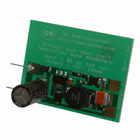
NCP1052GEVB
Manufacturer Part Number
NCP1052GEVB
Description
EVAL BOARD FOR NCP1052G
Manufacturer
ON Semiconductor
Specifications of NCP1052GEVB
Design Resources
NCP1052 Eval Board BOM NCP1052GEVB Gerber Files NCP1052 Demo Board Schematic
Main Purpose
AC/DC, Non-Isolated
Outputs And Type
1, Non-Isolated
Power - Output
1.2W
Voltage - Output
120V
Current - Output
100mA
Voltage - Input
85 ~ 265VAC
Regulator Topology
Boost, Buck
Frequency - Switching
136kHz
Board Type
Fully Populated
Utilized Ic / Part
NCP1052
Lead Free Status / RoHS Status
Lead free / RoHS Compliant
For Use With/related Products
NCP1052G
Other names
NCP1052GEVBOS


Pin Function Description
(SOT−223)
Pin
1
2
4
−
3
Control Input
(PDIP−8)
3, 7, 8
Pin
1
2
4
5
+
AC Line
Input
V
CC
1
2
No Connection
Power Switch
Control Input
Function
Ground
Drain
V
CC
Regulator Circuit
Startup & V
Fault Detector
Power Switch Circuit Output
Gating Logic
Oscillator &
This is the positive supply voltage input. During startup, power is supplied to this input
from Pin 5. When V
allowed to begin switching with 1.0 V hysteresis on the V
nected to this pin programs fault timing and frequency modulation rate.
The Power Switch Circuit is turned off when a current greater than approximately 50 mA
is drawn out of or applied to this pin. A 10 V clamp is built onto the chip to protect the
device from ESD damage or overvoltage conditions.
This pin is the control circuit and Power Switch Circuit ground. It is part of the integrated
circuit lead frame.
This pin is designed to directly drive the converter transformer primary, and internally
connects to Power Switch and Startup Circuit.
Figure 1. Typical Application
+
CC
http://onsemi.com
Ground
2
CC
reaches V
Snubber
Power
Switch
Circuit
3, 7−8
5
CC
(on), the Startup Circuit turns off and the output is
Description
+
CC
pin. The capacitance con-
Converter
DC Output
+
−
Related parts for NCP1052GEVB
Image
Part Number
Description
Manufacturer
Datasheet
Request
R

Part Number:
Description:
ON Semiconductor [VOLTAGE REGULATOR]
Manufacturer:
ON Semiconductor
Datasheet:
Part Number:
Description:
357-036-542-201 CARDEDGE 36POS DL .156 BLK LOPRO
Manufacturer:
ON Semiconductor
Datasheet:
Part Number:
Description:
357-036-542-201 CARDEDGE 36POS DL .156 BLK LOPRO
Manufacturer:
ON Semiconductor
Datasheet:
Part Number:
Description:
357-036-542-201 CARDEDGE 36POS DL .156 BLK LOPRO
Manufacturer:
ON Semiconductor
Datasheet:
Part Number:
Description:
357-036-542-201 CARDEDGE 36POS DL .156 BLK LOPRO
Manufacturer:
ON Semiconductor
Datasheet:
Part Number:
Description:
357-036-542-201 CARDEDGE 36POS DL .156 BLK LOPRO
Manufacturer:
ON Semiconductor
Datasheet:
Part Number:
Description:
357-036-542-201 CARDEDGE 36POS DL .156 BLK LOPRO
Manufacturer:
ON Semiconductor
Datasheet:
Part Number:
Description:
357-036-542-201 CARDEDGE 36POS DL .156 BLK LOPRO
Manufacturer:
ON Semiconductor
Datasheet:
Part Number:
Description:
357-036-542-201 CARDEDGE 36POS DL .156 BLK LOPRO
Manufacturer:
ON Semiconductor
Datasheet:
Part Number:
Description:
357-036-542-201 CARDEDGE 36POS DL .156 BLK LOPRO
Manufacturer:
ON Semiconductor
Datasheet:
Part Number:
Description:
357-036-542-201 CARDEDGE 36POS DL .156 BLK LOPRO
Manufacturer:
ON Semiconductor
Datasheet:
Part Number:
Description:
Manufacturer:
ON Semiconductor
Datasheet:
Part Number:
Description:
Manufacturer:
ON Semiconductor
Datasheet:
Part Number:
Description:
Manufacturer:
ON Semiconductor
Datasheet: