CDB4344 Cirrus Logic Inc, CDB4344 Datasheet - Page 2
CDB4344
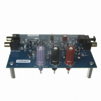
Manufacturer Part Number
CDB4344
Description
BOARD EVAL FOR CS4344 DAC
Manufacturer
Cirrus Logic Inc
Series
Popguard®r
Specifications of CDB4344
Number Of Dac's
2
Number Of Bits
24
Outputs And Type
2, Single Ended
Sampling Rate (per Second)
192k
Data Interface
Serial
Dac Type
Voltage
Voltage Supply Source
Analog and Digital
Operating Temperature
-10°C ~ 85°C
Utilized Ic / Part
CS4344
Description/function
Audio D/A
Operating Supply Voltage
5 V
Product
Audio Modules
For Use With/related Products
CS4344
Lead Free Status / RoHS Status
Contains lead / RoHS non-compliant
Lead Free Status / RoHS Status
Lead free / RoHS Compliant, Contains lead / RoHS non-compliant
Other names
598-1006


2
TABLE OF CONTENTS
1. PIN DESCRIPTIONS .............................................................................................................................. 4
2. CHARACTERISTICS AND SPECIFICATIONS ...................................................................................... 5
SPECIFIED OPERATING CONDITIONS ................................................................................................... 5
ABSOLUTE MAXIMUM RATINGS .............................................................................................................. 5
DAC ANALOG CHARACTERISTICS .......................................................................................................... 6
DAC ANALOG CHARACTERISTICS - ALL MODES .................................................................................. 6
COMBINED INTERPOLATION & ON-CHIP ANALOG FILTER RESPONSE ............................................. 7
DIGITAL INPUT CHARACTERISTICS ....................................................................................................... 8
POWER AND THERMAL CHARACTERISTICS ........................................................................................ 8
SWITCHING CHARACTERISTICS - SERIAL AUDIO INTERFACE ........................................................... 9
3. TYPICAL CONNECTION DIAGRAM ................................................................................................... 11
4. APPLICATIONS ................................................................................................................................... 12
5. FILTER PLOTS ..................................................................................................................................... 18
6. PARAMETER DEFINITIONS ................................................................................................................ 21
7. PACKAGE DIMENSIONS .................................................................................................................... 22
8. ORDERING INFORMATION ................................................................................................................ 23
9. REVISION HISTORY ............................................................................................................................ 24
4.1 Master Clock ................................................................................................................................. 12
4.2 Serial Clock .................................................................................................................................. 12
4.3 De-Emphasis ................................................................................................................................ 15
4.4 Initialization and Power-Down ...................................................................................................... 15
4.5 Output Transient Control .............................................................................................................. 15
4.6 Grounding and Power Supply Decoupling .................................................................................... 17
4.7 Analog Output and Filtering .......................................................................................................... 17
8.1 Functional Compatibility ............................................................................................................... 23
8.2 Selection Guide ............................................................................................................................ 23
4.2.1 External Serial Clock Mode ................................................................................................. 12
4.2.2 Internal Serial Clock Mode .................................................................................................. 12
4.5.1 Power-Up ............................................................................................................................ 15
4.5.2 Power-Down ........................................................................................................................ 15
CS4344/5/6/8
DS613F1
Related parts for CDB4344
Image
Part Number
Description
Manufacturer
Datasheet
Request
R

Part Number:
Description:
Development Kit
Manufacturer:
Cirrus Logic Inc
Datasheet:
Part Number:
Description:
Development Kit
Manufacturer:
Cirrus Logic Inc
Datasheet:


Part Number:
Description:
High-efficiency PFC + Fluorescent Lamp Driver Reference Design
Manufacturer:
Cirrus Logic Inc
Datasheet:
Part Number:
Description:
Development Kit
Manufacturer:
Cirrus Logic Inc
Datasheet:
Part Number:
Description:
Development Kit
Manufacturer:
Cirrus Logic Inc
Datasheet:

Part Number:
Description:
Development Kit
Manufacturer:
Cirrus Logic Inc
Datasheet:
Part Number:
Description:
Development Kit
Manufacturer:
Cirrus Logic Inc
Datasheet:
Part Number:
Description:
Development Kit
Manufacturer:
Cirrus Logic Inc
Datasheet:
Part Number:
Description:
Development Kit
Manufacturer:
Cirrus Logic Inc
Datasheet:

Part Number:
Description:
EVALUATION BOARD FOR CS8427
Manufacturer:
Cirrus Logic Inc
Datasheet:

Part Number:
Description:
BOARD EVAL FOR CS8416 RCVR
Manufacturer:
Cirrus Logic Inc
Datasheet:

Part Number:
Description:
EVALUATION BOARD FOR CS8420
Manufacturer:
Cirrus Logic Inc
Datasheet:

Part Number:
Description:
KIT DEVELOPMENT EP9315 ARM9
Manufacturer:
Cirrus Logic Inc
Datasheet:

Part Number:
Description:
KIT DEVELOPMENT EP9302 ARM9
Manufacturer:
Cirrus Logic Inc
Datasheet: