CDB4353 Cirrus Logic Inc, CDB4353 Datasheet - Page 5
CDB4353
Manufacturer Part Number
CDB4353
Description
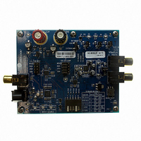
BOARD EVAL FOR CS4353 DAC
Manufacturer
Cirrus Logic Inc
Specifications of CDB4353
Number Of Dac's
2
Number Of Bits
24
Outputs And Type
2, Single Ended
Sampling Rate (per Second)
192k
Data Interface
Serial
Dac Type
Voltage
Voltage Supply Source
Single
Operating Temperature
-40°C ~ 85°C
Utilized Ic / Part
CS4353
Silicon Manufacturer
Cirrus Logic
Application Sub Type
DAC
Kit Application Type
Data Converter
Silicon Core Number
CS4353
Kit Contents
Board
Lead Free Status / RoHS Status
Contains lead / RoHS non-compliant
Lead Free Status / RoHS Status
Contains lead / RoHS non-compliant
Other names
598-1519
CDB-4353
CDB-4353


DS803DB2
5. POWER SUPPLY CIRCUITRY
Power is supplied to the evaluation board by two binding posts, GND and +3.3 V (see
input voltage range for the binding posts is 3.13 V to 3.47 V. The VL supply can be connected to the +3.3 V binding
post by shunting J1 or provided externally by removing the shunt on J1 and connecting another voltage to pin 2 of
J1 (labeled VL). VCP and VA are normally supplied by the 3.3 V binding post but can be set to separate voltages
by removing the shunts on J8 and J10, removing R9 and R14, and then applying external voltages to pin 1 of J8
and J10.
Power consumption of the CS4353 can be measured through the voltage drop at J8, J9, and J10 when the shunts
are removed.
6. GROUNDING AND POWER SUPPLY DECOUPLING
As with any high-performance converter, the CS4353 requires careful attention to power supply and grounding ar-
rangements to optimize performance.
show the component placement and top and bottom layout. The decoupling capacitors are located as close to the
CS4353 as possible.
7. HARDWARE CONTROL
The CDB4353 is controlled through settings on switch S1. This allows for configuration of the board without a PC.
Switch S1 can toggle settings for CS8416 MCLK speed, CS8416 and CS4353 PCM data format, clock and data
source for the board, and the Hardware Mode configuration of the CS4353.
S/PDIF input and PCM input header quick setup modes. See
8. CS8416 AND CS4353 RESET
Pressing switch S2 resets the CS8416. Jumper J5 sets whether the CS4353 is reset by switch S2 (External) or by
the CS4353’s internal power-on reset function (POR).
9. ANALOG OUTPUT FILTERING
The analog output on the CDB4353 has been designed according to the CS4353 datasheet. This output circuit con-
sists of a single-pole R and C filter. J11 selects the output ground reference for the CS4353. The output reference
can be set to the evaluation board’s ground (shunted) or J14 and J15’s ground connection (not shunted). See
Figure 33
WARNING: Refer to the CS4353 datasheet for maximum allowable voltages levels. Operation outside of this range
S1 POSITION
for details of CS4353 output filter.
can cause permanent damage to the device.
1
2
3
4
5
S/PDIF INPUT - OPT1 or J16
Figure 32
Table 1. Switch S1 Quick Setup
details the connections to the CS4353 and
Down
Down
Down
Up
Up
Table 4
for details on each switch S1 setting.
Table 1
PCM INPUT - J3
below shows S1 settings for
Figure
Down
Down
Down
Down
Figures
Up
33). The allowable
34, 35, and
CDB4353
36
5
Related parts for CDB4353
Image
Part Number
Description
Manufacturer
Datasheet
Request
R

Part Number:
Description:
Development Kit
Manufacturer:
Cirrus Logic Inc
Datasheet:
Part Number:
Description:
Development Kit
Manufacturer:
Cirrus Logic Inc
Datasheet:


Part Number:
Description:
High-efficiency PFC + Fluorescent Lamp Driver Reference Design
Manufacturer:
Cirrus Logic Inc
Datasheet:
Part Number:
Description:
Development Kit
Manufacturer:
Cirrus Logic Inc
Datasheet:
Part Number:
Description:
Development Kit
Manufacturer:
Cirrus Logic Inc
Datasheet:

Part Number:
Description:
Development Kit
Manufacturer:
Cirrus Logic Inc
Datasheet:
Part Number:
Description:
Development Kit
Manufacturer:
Cirrus Logic Inc
Datasheet:
Part Number:
Description:
Development Kit
Manufacturer:
Cirrus Logic Inc
Datasheet:
Part Number:
Description:
Development Kit
Manufacturer:
Cirrus Logic Inc
Datasheet:

Part Number:
Description:
EVALUATION BOARD FOR CS8427
Manufacturer:
Cirrus Logic Inc
Datasheet:

Part Number:
Description:
BOARD EVAL FOR CS8416 RCVR
Manufacturer:
Cirrus Logic Inc
Datasheet:

Part Number:
Description:
EVALUATION BOARD FOR CS8420
Manufacturer:
Cirrus Logic Inc
Datasheet:

Part Number:
Description:
KIT DEVELOPMENT EP9315 ARM9
Manufacturer:
Cirrus Logic Inc
Datasheet:

Part Number:
Description:
KIT DEVELOPMENT EP9302 ARM9
Manufacturer:
Cirrus Logic Inc
Datasheet: