CDB4353 Cirrus Logic Inc, CDB4353 Datasheet
CDB4353
Specifications of CDB4353
CDB-4353


Related parts for CDB4353


CDB4353 Summary of contents
Page 1
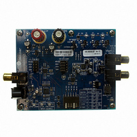
... Full-scale Output The CS4353 is available in a 24-pin QFN package in Commercial (-40°C to +85°C) grade. The CDB4353 Customer Demonstration Board is also available for de- vice evaluation and implementation suggestions. Please see plete details. ...
Page 2
TABLE OF CONTENTS 1. PIN DESCRIPTIONS ............................................................................................................................. 4 2. CHARACTERISTICS AND SPECIFICATIONS ...................................................................................... 6 RECOMMENDED OPERATING CONDITIONS .................................................................................... 6 ABSOLUTE MAXIMUM RATINGS ........................................................................................................ 6 DAC ANALOG CHARACTERISTICS .................................................................................................... 7 COMBINED INTERPOLATION & ON-CHIP ANALOG FILTER RESPONSE ........................................ 8 SWITCHING SPECIFICATIONS ...
Page 3
LIST OF FIGURES Figure 1.Serial Input Timing ........................................................................................................................ 9 Figure 2.Power-on Reset Threshold Sequence ........................................................................................ 10 Figure 3.Typical Connection Diagram ....................................................................................................... 12 Figure 4.Stereo Pseudo-differential Output ............................................................................................... 13 Figure 5.I² 24-bit Data ................................................................................................................... 15 Figure 6.Left-justified up to ...
Page 4
PIN DESCRIPTIONS SCLK MCLK VL DGND FLYP- VCP Pin Name Pin # SCLK 1 Serial Clock (Input) - Serial clock for the serial audio interface. MCLK 2 Master Clock (Input) - Clock source for the delta-sigma modulator and digital ...
Page 5
VA 17 Low Voltage Analog Power (Input) - Positive power supply for the analog section. VBIAS 18 Positive Voltage Reference (Output) - Positive reference voltage for the internal DAC. Reset (Input) - Optional connection for an external reset control. The ...
Page 6
CHARACTERISTICS AND SPECIFICATIONS RECOMMENDED OPERATING CONDITIONS AGND = DNGD = CPGND = 0 V; all voltages with respect to ground. Parameters DC Power Supply Charge Pump and Digital Core power Low Voltage Analog power Ambient Operating Temperature (Power Applied) ...
Page 7
DAC ANALOG CHARACTERISTICS Test conditions (unless otherwise specified): T CPGND = 0 V; VBIAS, VFILT+/-, and FLYP/N+/- capacitors as shown in 997 Hz sine wave at 0 dBFS; measurement bandwidth kHz. Parameter Dynamic Performance ...
Page 8
SDIN = 0. AOUT_REF input test signal Hz, 50 mVpp sine wave. Measured by applying the test signal into the AOUT_REF pin and measuring the resulting output amplitude on the AOUTx pin. Spec- ification calculated by: ...
Page 9
SWITCHING SPECIFICATIONS - SERIAL AUDIO INTERFACE Parameters MCLK Frequency MCLK Duty Cycle Input Sample Rate (Auto selection) LRCK Duty Cycle SCLK Pulse Width Low SCLK Pulse Width High SCLK Period SCLK rising to LRCK edge delay SCLK rising to LRCK ...
Page 10
DIGITAL INTERFACE CHARACTERISTICS Test conditions (unless otherwise specified): AGND = DGND = CPGND = 0 V; all voltages with respect to ground. Parameters High-Level Input Voltage Low-Level Input Voltage Input Leakage Current Input Capacitance INTERNAL POWER-ON RESET THRESHOLD VOLTAGES Test ...
Page 11
DC ELECTRICAL CHARACTERISTICS Test conditions (unless otherwise specified): VCP = 3.3 V; AGND = DGND = CPGND = 0 V; SDIN = 0; all voltages with respect to ground. Parameters Power Supplies Power Supply Current (Note ...
Page 12
TYPICAL CONNECTION DIAGRAM +3 2.2 µF Digital Audio Processor +0 +3.3 V 0.1 µF Note 2 Hardware Control Note 2:Connect RESET internal power-on reset is used. 12 0.1 µF 0.1 µF 6 ...
Page 13
APPLICATIONS 4.1 Line Outputs 4.1.1 Ground-centered Outputs An on-chip charge pump creates both positive and negative high-voltage supplies, which allows the full- scale output swing to be centered around ground. This eliminates the need for large DC-blocking capac- itors ...
Page 14
Sample Rate Range/Operational Mode Detect The CS4353 operates in one of three operational modes. The device will auto-detect the correct mode when the input sample rate (Fs), defined by the LRCK frequency, falls within one of the ranges illustrated ...
Page 15
Digital Interface Format The device will accept audio samples in either I²S or Left-Justified digital interface formats, as illustrated in Table 6. The desired format is selected via the I²S/LJ pin. For an illustration of the required relationship between ...
Page 16
De-emphasis Control The device includes on-chip digital de-emphasis. 44.1 kHz. The frequency response of the de-emphasis curve scales with changes in the sample rate, Fs. The de-emphasis error will increase for sample rates other than 44.1 kHz. When the ...
Page 17
Initialization When power is first applied, the DAC enters a reset (low power) state at the beginning of the initialization sequence. In this state, the AOUTx pins are weakly pulled to ground and VBIAS is connected to VA. The ...
Page 18
USER: Change MCLK/LRCK ratio Valid MCLK/LRCK Ratio Figure 9. Initialization and Power-down Sequence Diagram 18 USER: Apply Power Reset State Outputs Grounded USER: RESET Set High or RESET Tied High (if using POR) Power-Down State USER: Apply MCLK Initialization State ...
Page 19
Recommended Power-up and Power-down Sequences 4.9.1 Power-up Sequences 4.9.1.1 External RESET Power-up Sequence Follow the power-up sequence below if the external RESET pin is used: 1. Hold RESET low while the power supplies are turned on. 2. Set the ...
Page 20
... See voltage present across pin pairs. This is useful for choosing appropriate capacitor voltage ratings and ori- entation if electrolytic capacitors are used. The CDB4353 evaluation board demonstrates the optimum layout and power supply arrangements. 20 CS4353 ...
Page 21
DIGITAL FILTER RESPONSE PLOTS 0 −20 −40 −60 −80 −100 −120 0.4 0.5 0.6 0.7 Frequency(normalized to Fs) Figure 10. Single-speed Stopband Rejection 0 −1 −2 −3 −4 −5 −6 −7 −8 −9 −10 0.45 0.46 0.47 0.48 0.49 ...
Page 22
Frequency(normalized to Fs) Figure 16. Double-speed Transition Band (detail 100 120 0.2 0.3 0.4 0.5 0.6 Frequency(normalized ...
Page 23
PARAMETER DEFINITIONS Total Harmonic Distortion + Noise (THD+N) The ratio of the RMS value of the signal to the RMS sum of all other spectral components over the specified bandwidth (typically kHz), including distortion components. ...
Page 24
PACKAGE DIMENSIONS 24L QFN (4.00 mm BODY) PACKAGE DRAWING D 1.00 REF PIN #1 IDENTIFIER LASER MARKING TOP VIEW INCHES DIM MIN 0.00000 b 0.00787 0.00984 e 0.01772 0.01969 D 0.15748 BSC D2 0.10433 0.10630 E ...
Page 25
... DAC Analog Characteristics Internal Power-on Reset Threshold Voltages Filter. CS4353 Temp Range Container Order # Rail CS4353-CNZ -40° to +85° C Tape & Reel CS4353-CNZR - - CDB4353 specification table. DC Electrical Characteristics table. table. specification table. DAC Analog Characteristics table. table. table. table. table. 25 ...
Page 26
Contacting Cirrus Logic Support For all product questions and inquiries, contact a Cirrus Logic Sales Representative. To find one nearest you www.cirrus.com. IMPORTANT NOTICE Cirrus Logic, Inc. and its subsidiaries (“Cirrus”) believe that the information contained in this ...