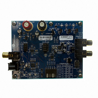
CDB4353 Cirrus Logic Inc, CDB4353 Datasheet - Page 13

CDB4353
Manufacturer Part Number
CDB4353
Description
BOARD EVAL FOR CS4353 DAC
Manufacturer
Cirrus Logic Inc
Specifications of CDB4353
Number Of Dac's
2
Number Of Bits
24
Outputs And Type
2, Single Ended
Sampling Rate (per Second)
192k
Data Interface
Serial
Dac Type
Voltage
Voltage Supply Source
Single
Operating Temperature
-40°C ~ 85°C
Utilized Ic / Part
CS4353
Silicon Manufacturer
Cirrus Logic
Application Sub Type
DAC
Kit Application Type
Data Converter
Silicon Core Number
CS4353
Kit Contents
Board
Lead Free Status / RoHS Status
Contains lead / RoHS non-compliant
Lead Free Status / RoHS Status
Contains lead / RoHS non-compliant
Other names
598-1519
CDB-4353
CDB-4353
DS803F1
4. APPLICATIONS
4.1
4.1.1
4.1.2
4.1.3
Line Outputs
Ground-centered Outputs
An on-chip charge pump creates both positive and negative high-voltage supplies, which allows the full-
scale output swing to be centered around ground. This eliminates the need for large DC-blocking capac-
itors which create audible pops at power-on, allows the CS4353 to deliver a larger full-scale output at low-
er supply voltages, and provides improved bandwidth frequency response.
Full-scale Output Amplitude Control
The full-scale output voltage amplitude is selected via the 1_2VRMS pin. When the pin is connected to
VL, the full-scale output voltage at the AOUTx pins is approximately 2 V
to GND, the full-scale output voltage at the AOUTx pins is approximately 1 V
between the AOUTx pin and the load will lower the voltage delivered to the load. See the
Characteristics
Pseudo-differential Outputs
The CS4353 implements a pseudo-differential output stage. The AOUT_REF input is intended to be used
as a pseudo-differential reference signal. This feature provides common mode noise rejection with single-
ended signals.
ential output stage, including a recommended stereo pseudo-differential output topology. If pseudo-differ-
ential output functionality is not required, simply connect the AOUT_REF pin to ground next to the
CS4353. If a split-ground design is used, the AOUT_REF pin should be connected to AGND. See the
solute Maximum Ratings
voltage on the AOUT_REF pin will cause a DC offset on the DAC output.
Internal Right
Internal Left
DAC Signal
DAC Signal
Figure 4
table for the complete specifications of the full-scale output voltage.
Figure 4. Stereo Pseudo-differential Output
shows a basic diagram outlining the internal implementation of the pseudo-differ-
table for the maximum allowable voltage on the AOUT_REF pin. Applying a DC
AOUTA
AOUT_REF
AOUTB
mode rejection, reducing external system noise
Psuedo-differential output improves common
RMS
. When the pin is connected
(pseudo-differential traces)
(pseudo-differential traces)
RMS
. Additional impedance
//
//
//
Left Output
Right Output
DAC Analog
CS4353
GND
Ab-
13


