CDB4353 Cirrus Logic Inc, CDB4353 Datasheet - Page 17
CDB4353
Manufacturer Part Number
CDB4353
Description
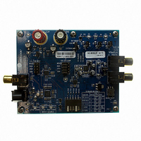
BOARD EVAL FOR CS4353 DAC
Manufacturer
Cirrus Logic Inc
Specifications of CDB4353
Number Of Dac's
2
Number Of Bits
24
Outputs And Type
2, Single Ended
Sampling Rate (per Second)
192k
Data Interface
Serial
Dac Type
Voltage
Voltage Supply Source
Single
Operating Temperature
-40°C ~ 85°C
Utilized Ic / Part
CS4353
Silicon Manufacturer
Cirrus Logic
Application Sub Type
DAC
Kit Application Type
Data Converter
Silicon Core Number
CS4353
Kit Contents
Board
Lead Free Status / RoHS Status
Contains lead / RoHS non-compliant
Lead Free Status / RoHS Status
Contains lead / RoHS non-compliant
Other names
598-1519
CDB-4353
CDB-4353


CS4353
4.8
Initialization
When power is first applied, the DAC enters a reset (low power) state at the beginning of the initialization
sequence. In this state, the AOUTx pins are weakly pulled to ground and VBIAS is connected to VA.
The device will remain in the reset state until the RESET pin is brought high. Once the RESET pin is high,
the internal digital circuitry is reset and the DAC enters a power-down state until MCLK is applied. Alterna-
tively, if no external reset control is required, the internal power-on reset can be used by tying the RESET
pin to VL (see
Section
4.7).
Once MCLK is valid, the device enters an initialization state in which the charge pump powers up and charg-
es the capacitors for both the positive and negative high-voltage supplies.
Once LRCK and SCLK are valid, the number of MCLK cycles is counted relative to the LRCK period to de-
termine the MCLK/LRCK frequency ratio. Next, the device enters the power-up state in which the interpo-
lation and decimation filters and delta-sigma modulators are turned on, the internal voltage reference,
VBIAS, powers up to normal operation, the analog output pull-down resistors are removed, and power is
applied to the output amplifiers.
After this power-up state sequence is complete, normal operation begins and analog output is generated.
If valid MCLK, LRCK, and SCLK are applied to the DAC before RESET is set high, the total time from RE-
SET being set high to the analog audio output from AOUTx is less than 50 ms.
See
Figure 9
for a diagram of the device’s states and transition conditions.
DS803F1
17
Related parts for CDB4353
Image
Part Number
Description
Manufacturer
Datasheet
Request
R

Part Number:
Description:
Development Kit
Manufacturer:
Cirrus Logic Inc
Datasheet:
Part Number:
Description:
Development Kit
Manufacturer:
Cirrus Logic Inc
Datasheet:


Part Number:
Description:
High-efficiency PFC + Fluorescent Lamp Driver Reference Design
Manufacturer:
Cirrus Logic Inc
Datasheet:
Part Number:
Description:
Development Kit
Manufacturer:
Cirrus Logic Inc
Datasheet:
Part Number:
Description:
Development Kit
Manufacturer:
Cirrus Logic Inc
Datasheet:

Part Number:
Description:
Development Kit
Manufacturer:
Cirrus Logic Inc
Datasheet:
Part Number:
Description:
Development Kit
Manufacturer:
Cirrus Logic Inc
Datasheet:
Part Number:
Description:
Development Kit
Manufacturer:
Cirrus Logic Inc
Datasheet:
Part Number:
Description:
Development Kit
Manufacturer:
Cirrus Logic Inc
Datasheet:

Part Number:
Description:
EVALUATION BOARD FOR CS8427
Manufacturer:
Cirrus Logic Inc
Datasheet:

Part Number:
Description:
BOARD EVAL FOR CS8416 RCVR
Manufacturer:
Cirrus Logic Inc
Datasheet:

Part Number:
Description:
EVALUATION BOARD FOR CS8420
Manufacturer:
Cirrus Logic Inc
Datasheet:

Part Number:
Description:
KIT DEVELOPMENT EP9315 ARM9
Manufacturer:
Cirrus Logic Inc
Datasheet:

Part Number:
Description:
KIT DEVELOPMENT EP9302 ARM9
Manufacturer:
Cirrus Logic Inc
Datasheet: