CDB4353 Cirrus Logic Inc, CDB4353 Datasheet - Page 4
CDB4353
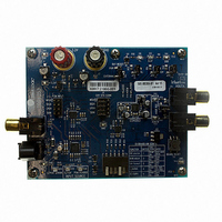
Manufacturer Part Number
CDB4353
Description
BOARD EVAL FOR CS4353 DAC
Manufacturer
Cirrus Logic Inc
Specifications of CDB4353
Number Of Dac's
2
Number Of Bits
24
Outputs And Type
2, Single Ended
Sampling Rate (per Second)
192k
Data Interface
Serial
Dac Type
Voltage
Voltage Supply Source
Single
Operating Temperature
-40°C ~ 85°C
Utilized Ic / Part
CS4353
Silicon Manufacturer
Cirrus Logic
Application Sub Type
DAC
Kit Application Type
Data Converter
Silicon Core Number
CS4353
Kit Contents
Board
Lead Free Status / RoHS Status
Contains lead / RoHS non-compliant
Lead Free Status / RoHS Status
Contains lead / RoHS non-compliant
Other names
598-1519
CDB-4353
CDB-4353


4
1. PIN DESCRIPTIONS
SCLK
MCLK
VL
DGND
FLYP+
FLYP-
VCP
VFILT+
FLYN+
FLYN-
CPGND
VFILT-
AOUTB
AOUTA
AOUT_REF
AGND
Pin Name Pin #
11
10
12
13
15
14
16
1
2
3
4
7
5
6
8
9
Serial Clock (Input) - Serial clock for the serial audio interface.
Master Clock (Input) - Clock source for the delta-sigma modulator and digital filters.
Serial Audio Interface Power (Input) - Positive power for the serial audio interface
Digital Ground (Input) - Ground reference for the digital section.
Step-up Charge Pump Cap Positive/Negative Nodes (Output) - Positive and Negative nodes for the
step-up charge pump’s flying capacitor.
Charge Pump and Digital Core Logic Power (Input) - Positive power supply for the step-up and invert-
ing charge pumps as well as the digital core logic sections.
Step-up Charge Pump Filter Connection (Output) - Power supply from the step-up charge pump that
provides the positive rail for the output amplifiers
Inverting Charge Pump Cap Positive/Negative Nodes (Output) - Positive and Negative nodes for the
inverting charge pump’s flying capacitor.
Charge Pump Ground (Input) - Ground reference for the Charge Pump section.
Inverting Charge Pump Filter Connection (Output) - Power supply from the inverting charge pump that
provides the negative rail for the output amplifiers.
Analog Outputs (Output) - The full-scale analog line output level is specified in the Analog Characteris-
tics table.
Pseudo Diff. Analog Output Reference (Input) - Ground reference for the analog output amplifiers.
This pin must be at the same nominal DC voltage as the AGND pin.
Analog Ground (Input) - Ground reference for the low voltage analog section.
DGND
FLYP-
MCLK
SCLK
VCP
VL
1
3
5
2
4
6
24
7
Top-Down (Through Package) View
23
8
24-Pin QFN Package
Thermal Pad
22
9
Pin Description
21
10
20
11
19
12
18
17
16
15
14
13
VBIAS
VA
AGND
AOUTA
AOUT_REF
AOUTB
CS4353
DS803F1
Related parts for CDB4353
Image
Part Number
Description
Manufacturer
Datasheet
Request
R

Part Number:
Description:
Development Kit
Manufacturer:
Cirrus Logic Inc
Datasheet:
Part Number:
Description:
Development Kit
Manufacturer:
Cirrus Logic Inc
Datasheet:


Part Number:
Description:
High-efficiency PFC + Fluorescent Lamp Driver Reference Design
Manufacturer:
Cirrus Logic Inc
Datasheet:
Part Number:
Description:
Development Kit
Manufacturer:
Cirrus Logic Inc
Datasheet:
Part Number:
Description:
Development Kit
Manufacturer:
Cirrus Logic Inc
Datasheet:

Part Number:
Description:
Development Kit
Manufacturer:
Cirrus Logic Inc
Datasheet:
Part Number:
Description:
Development Kit
Manufacturer:
Cirrus Logic Inc
Datasheet:
Part Number:
Description:
Development Kit
Manufacturer:
Cirrus Logic Inc
Datasheet:
Part Number:
Description:
Development Kit
Manufacturer:
Cirrus Logic Inc
Datasheet:

Part Number:
Description:
EVALUATION BOARD FOR CS8427
Manufacturer:
Cirrus Logic Inc
Datasheet:

Part Number:
Description:
BOARD EVAL FOR CS8416 RCVR
Manufacturer:
Cirrus Logic Inc
Datasheet:

Part Number:
Description:
EVALUATION BOARD FOR CS8420
Manufacturer:
Cirrus Logic Inc
Datasheet:

Part Number:
Description:
KIT DEVELOPMENT EP9315 ARM9
Manufacturer:
Cirrus Logic Inc
Datasheet:

Part Number:
Description:
KIT DEVELOPMENT EP9302 ARM9
Manufacturer:
Cirrus Logic Inc
Datasheet: