CDB4353 Cirrus Logic Inc, CDB4353 Datasheet - Page 11
CDB4353
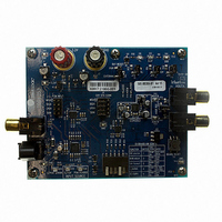
Manufacturer Part Number
CDB4353
Description
BOARD EVAL FOR CS4353 DAC
Manufacturer
Cirrus Logic Inc
Specifications of CDB4353
Number Of Dac's
2
Number Of Bits
24
Outputs And Type
2, Single Ended
Sampling Rate (per Second)
192k
Data Interface
Serial
Dac Type
Voltage
Voltage Supply Source
Single
Operating Temperature
-40°C ~ 85°C
Utilized Ic / Part
CS4353
Silicon Manufacturer
Cirrus Logic
Application Sub Type
DAC
Kit Application Type
Data Converter
Silicon Core Number
CS4353
Kit Contents
Board
Lead Free Status / RoHS Status
Contains lead / RoHS non-compliant
Lead Free Status / RoHS Status
Contains lead / RoHS non-compliant
Other names
598-1519
CDB-4353
CDB-4353


DS803F1
DC ELECTRICAL CHARACTERISTICS
Test conditions (unless otherwise specified): VCP = VA = VL = 3.3 V; AGND = DGND = CPGND = 0 V; SDIN = 0;
all voltages with respect to ground.
Notes: 15. Current consumption increases with increasing sample rate and increasing MCLK frequency. Typical
2.1
Power Supplies
Power Supply Current
Power Dissipation (All Supplies)
(Note 15)
Power Supply Rejection Ratio
DC Output Voltages
Pin Voltage
16. Power-down is defined as RESET pin = Low with all clock and data lines held static low. All digital inputs
17. Valid with the recommended capacitor value on VBIAS as shown in the typical connection diagram in
18. Typical voltage shown for “Initialization State”, see
Digital I/O Pin Characteristics
Input and output levels and associated power supply voltage are shown in
exceed the corresponding power supply voltage.
Pin Name
1_2VRMS
values are based on Fs = 48 kHz and MCLK = 12.288 MHz. Maximum values are based on highest
sample rate and highest MCLK frequency; see
ance between speed modes is small.
have a weak pull-down (approximately 50 kΩ) which is only present during reset. Opposing this pull-
down will slightly increase the power-down current.
Section
during normal operation.
RESET
MCLK
LRCK
SCLK
I²S/LJ
SDIN
DEM
3.
(Note 15)
Power Supply
Parameters
(Note 17)
Power-Down, All Supplies
VL
Normal Operation, 1_2VRMS = 0
Table 1. Digital I/O Pin Characteristics
VFILT+ to GND
GND to VFILT-
Power-Down
Normal Operation
Input
Input
Input
Input
Input
Input
Input
Input
FLYN+ to FLYN-
FLYP+ to FLYP-
I/O
VA to VBIAS
(Note 16)
(Note 16)
(Note 18)
(Note 18)
(1 kHz)
(60 Hz)
Switching Specifications - Serial Audio
Section
Symbol
PSRR
Driver
I
VCP
I
I
I
PD
VA
VL
-
-
-
-
-
-
-
-
4.8. Typical voltage may be up to 1.5 V lower
Min
-
-
-
-
-
-
-
-
-
-
-
-
-
Table
0.9 V - 3.3 V, with Hysteresis
Typ
127
2.4
0.1
3.3
6.6
6.6
6.6
2.1
36
65
60
60
1
1. Logic levels should not
0.9 V - 3.3 V
0.9 V - 3.3 V
0.9 V - 3.3 V
0.9 V - 3.3 V
0.9 V - 3.3 V
0.9 V - 3.3 V
0.9 V - 3.3 V
Receiver
Max
152
0.2
43
3
-
-
-
-
-
-
-
-
-
Interface. Vari-
CS4353
Units
mW
mW
mA
mA
mA
μA
dB
dB
V
V
V
V
V
11
Related parts for CDB4353
Image
Part Number
Description
Manufacturer
Datasheet
Request
R

Part Number:
Description:
Development Kit
Manufacturer:
Cirrus Logic Inc
Datasheet:
Part Number:
Description:
Development Kit
Manufacturer:
Cirrus Logic Inc
Datasheet:


Part Number:
Description:
High-efficiency PFC + Fluorescent Lamp Driver Reference Design
Manufacturer:
Cirrus Logic Inc
Datasheet:
Part Number:
Description:
Development Kit
Manufacturer:
Cirrus Logic Inc
Datasheet:
Part Number:
Description:
Development Kit
Manufacturer:
Cirrus Logic Inc
Datasheet:

Part Number:
Description:
Development Kit
Manufacturer:
Cirrus Logic Inc
Datasheet:
Part Number:
Description:
Development Kit
Manufacturer:
Cirrus Logic Inc
Datasheet:
Part Number:
Description:
Development Kit
Manufacturer:
Cirrus Logic Inc
Datasheet:
Part Number:
Description:
Development Kit
Manufacturer:
Cirrus Logic Inc
Datasheet:

Part Number:
Description:
EVALUATION BOARD FOR CS8427
Manufacturer:
Cirrus Logic Inc
Datasheet:

Part Number:
Description:
BOARD EVAL FOR CS8416 RCVR
Manufacturer:
Cirrus Logic Inc
Datasheet:

Part Number:
Description:
EVALUATION BOARD FOR CS8420
Manufacturer:
Cirrus Logic Inc
Datasheet:

Part Number:
Description:
KIT DEVELOPMENT EP9315 ARM9
Manufacturer:
Cirrus Logic Inc
Datasheet:

Part Number:
Description:
KIT DEVELOPMENT EP9302 ARM9
Manufacturer:
Cirrus Logic Inc
Datasheet: