CDB4353 Cirrus Logic Inc, CDB4353 Datasheet - Page 19
CDB4353
Manufacturer Part Number
CDB4353
Description
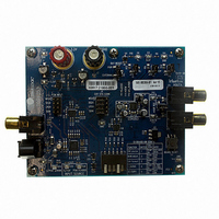
BOARD EVAL FOR CS4353 DAC
Manufacturer
Cirrus Logic Inc
Specifications of CDB4353
Number Of Dac's
2
Number Of Bits
24
Outputs And Type
2, Single Ended
Sampling Rate (per Second)
192k
Data Interface
Serial
Dac Type
Voltage
Voltage Supply Source
Single
Operating Temperature
-40°C ~ 85°C
Utilized Ic / Part
CS4353
Silicon Manufacturer
Cirrus Logic
Application Sub Type
DAC
Kit Application Type
Data Converter
Silicon Core Number
CS4353
Kit Contents
Board
Lead Free Status / RoHS Status
Contains lead / RoHS non-compliant
Lead Free Status / RoHS Status
Contains lead / RoHS non-compliant
Other names
598-1519
CDB-4353
CDB-4353


DS803F1
4.9
4.9.1
4.9.2
Recommended Power-up and Power-down Sequences
4.9.1.1
Follow the power-up sequence below if the external RESET pin is used:
4.9.1.2
Follow the power-up sequence below if the internal power-on reset is used:
4.9.2.1
Follow the power-down sequence below if the external RESET pin is used:
4.9.2.2
Follow the power-down sequence below if the internal power-on reset is used:
Power-up Sequences
1. Hold RESET low while the power supplies are turned on.
2. Set the I²S/LJ, 1_2VRMS, and DEM configuration pins to the desired state.
3. Provide the correct MCLK, LRCK, and SCLK signals locked to the appropriate frequencies as
4. After the power supplies, configuration pins, and clock signals are stable, bring RESET high. The
1. Hold RESET high (connected to VL) while the power supplies are turned on. The power-on reset
2. Set the I²S/LJ, 1_2VRMS, and DEM configuration pins to the desired state.
3. After the power supplies and configuration pins are stable, provide the correct MCLK, LRCK, and
Power-down Sequences
1. For minimal pops, set the input digital data to zero for at least 8192 consecutive samples.
2. Bring RESET low.
3. Remove the power supply voltages.
1. For minimal pops, set the input digital data to zero for at least 8192 consecutive samples.
2. Remove the MCLK signal without applying any glitched pulses to the MCLK pin.
3. Remove the power supply voltages.
Note:
MCLK signal duty cycle specification and the nominal frequency of the input MCLK signal. A transient may
occur on the analog outputs if the MCLK signal duty cycle specification is violated when the MCLK signal
is removed during normal operation; see
discussed in
device will initiate the power-up sequence seen in
will be output from AOUTx within 50 ms after RESET is set high.
circuitry will function as described in
SCLK signals to progress from the ‘Power-Down State’ in the power-up sequence seen in
The sequence will complete and audio will be output from the AOUTx pins within 50 ms after valid
clocks are applied.
A glitched pulse is any pulse that is shorter than the period defined by the minimum/maximum
External RESET Power-up Sequence
Internal Power-on Reset Power-up Sequence
External RESET Power-down Sequence
Internal Power-on Reset Power-down Sequence
Section
4.3.
Section
“Switching Specifications - Serial Audio Interface” on page
4.7.
Figure
9. The sequence will complete and audio
CS4353
Figure
9.
9.
19
Related parts for CDB4353
Image
Part Number
Description
Manufacturer
Datasheet
Request
R

Part Number:
Description:
Development Kit
Manufacturer:
Cirrus Logic Inc
Datasheet:
Part Number:
Description:
Development Kit
Manufacturer:
Cirrus Logic Inc
Datasheet:


Part Number:
Description:
High-efficiency PFC + Fluorescent Lamp Driver Reference Design
Manufacturer:
Cirrus Logic Inc
Datasheet:
Part Number:
Description:
Development Kit
Manufacturer:
Cirrus Logic Inc
Datasheet:
Part Number:
Description:
Development Kit
Manufacturer:
Cirrus Logic Inc
Datasheet:

Part Number:
Description:
Development Kit
Manufacturer:
Cirrus Logic Inc
Datasheet:
Part Number:
Description:
Development Kit
Manufacturer:
Cirrus Logic Inc
Datasheet:
Part Number:
Description:
Development Kit
Manufacturer:
Cirrus Logic Inc
Datasheet:
Part Number:
Description:
Development Kit
Manufacturer:
Cirrus Logic Inc
Datasheet:

Part Number:
Description:
EVALUATION BOARD FOR CS8427
Manufacturer:
Cirrus Logic Inc
Datasheet:

Part Number:
Description:
BOARD EVAL FOR CS8416 RCVR
Manufacturer:
Cirrus Logic Inc
Datasheet:

Part Number:
Description:
EVALUATION BOARD FOR CS8420
Manufacturer:
Cirrus Logic Inc
Datasheet:

Part Number:
Description:
KIT DEVELOPMENT EP9315 ARM9
Manufacturer:
Cirrus Logic Inc
Datasheet:

Part Number:
Description:
KIT DEVELOPMENT EP9302 ARM9
Manufacturer:
Cirrus Logic Inc
Datasheet: