EVAL-AD5429EBZ Analog Devices Inc, EVAL-AD5429EBZ Datasheet - Page 14
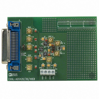
EVAL-AD5429EBZ
Manufacturer Part Number
EVAL-AD5429EBZ
Description
BOARD EVALUATION FOR AD5429
Manufacturer
Analog Devices Inc
Specifications of EVAL-AD5429EBZ
Number Of Dac's
2
Number Of Bits
8
Outputs And Type
2, Single Ended
Sampling Rate (per Second)
2.47M
Data Interface
Serial
Settling Time
30ns
Dac Type
Current
Voltage Supply Source
Single
Operating Temperature
-40°C ~ 125°C
Utilized Ic / Part
AD5429
Lead Free Status / RoHS Status
Lead free / RoHS Compliant


AD5429/AD5439/AD5449
TERMINOLOGY
Relative Accuracy (Endpoint Nonlinearity)
A measure of the maximum deviation from a straight line
passing through the endpoints of the DAC transfer function.
It is measured after adjusting for zero and full scale and is typically
expressed in LSBs or as a percentage of the full-scale reading.
Differential Nonlinearity
The difference in the measured change and the ideal 1 LSB
change between two adjacent codes. A specified differential
nonlinearity of −1 LSB maximum over the operating temperature
range ensures monotonicity.
Gain Error (Full-Scale Error)
A measure of the output error between an ideal DAC and the
actual device output. For these DACs, ideal maximum output is
V
with an external resistance.
Output Leakage Current
The current that flows into the DAC ladder switches when they
are turned off. For the I
loading all 0s to the DAC and measuring the I
Minimum current flows into the I
loaded with all 1s.
Output Capacitance
Capacitance from I
Output Current Settling Time
The amount of time for the output to settle to a specified level
for a full-scale input change. For these devices, it is specified
with a 100 Ω resistor to ground.
Digital-to-Analog Glitch Impulse
The amount of charge injected from the digital inputs to the
analog output when the inputs change state. This is normally
specified as the area of the glitch in either pA-sec or nV-sec,
depending on whether the glitch is measured as a current or
voltage signal.
Digital Feedthrough
When the device is not selected, high frequency logic activity
on the digital inputs of the device is capacitively coupled through
the device and produces noise on the I
on the circuitry that follows. This noise is digital feedthrough.
Multiplying Feedthrough Error
The error due to capacitive feedthrough from the DAC
reference input to the DAC I
loaded to the DAC.
REF
− 1 LSB. The gain error of the DACs is adjustable to zero
OUT
1 or I
OUT
1x terminal, it can be measured by
OUT
OUT
2 to AGND.
1x terminal when all 0s are
OUT
OUT
2x line when the DAC is
pins and, subsequently,
OUT
1 current.
Rev. C | Page 14 of 32
Digital Crosstalk
The glitch impulse transferred to the outputs of one DAC in
response to a full-scale code change (all 0s to all 1s, or vice versa)
in the input register of the other DAC. It is expressed in nV-sec.
Analog Crosstalk
The glitch impulse transferred to the output of one DAC due to
a change in the output of another DAC. It is measured by
loading one of the input registers with a full-scale code change
(all 0s to all 1s, or vice versa) while keeping LDAC high and
then pulsing LDAC low and monitoring the output of the DAC
whose digital code has not changed. The area of the glitch is
expressed in nV-sec.
Channel-to-Channel Isolation
The portion of input signal from the reference input of a DAC
that appears at the output of another DAC. It is expressed in dB.
Total Harmonic Distortion (THD)
The DAC is driven by an ac reference. The ratio of the rms sum
of the harmonics of the DAC output to the fundamental value is
the THD. Usually only the lower-order harmonics are included,
such as the second to fifth harmonics.
Intermodulation Distortion (IMD)
The DAC is driven by two combined sine wave references of
Frequency fa and Frequency fb. Distortion products are produced
at sum and difference frequencies of mfa ± nfb, where m, n = 0, 1,
2, 3 … Intermodulation terms are those for which m or n is not
equal to 0. The second-order terms include (fa + fb) and (fa − fb),
and the third-order terms are (2fa + fb), (2fa − fb), (f + 2fa + 2fb),
and (fa − 2fb). IMD is defined as
Compliance Voltage Range
The maximum range of (output) terminal voltage for which the
device provides the specified characteristics.
IMD
THD
=
20
log
=
20
RMS
log
Sum
V
RMS
2
2
of
+
V
Amplitude
the
3
2
V
+
1
Sum
V
4
2
and
+
of
V
5
Diff
the
2
Fundamenta
Distortion
Products
l
Related parts for EVAL-AD5429EBZ
Image
Part Number
Description
Manufacturer
Datasheet
Request
R


Part Number:
Description:
BOARD EVAL FOR SI270X-A
Manufacturer:
Silicon Laboratories Inc
Datasheet:

Part Number:
Description:
BUCK CONV REF DESIGN KIT IP1201
Manufacturer:
International Rectifier
Datasheet:
Part Number:
Description:
BOARD DEMO SYNC DUAL BUCK CNVTER
Manufacturer:
International Rectifier
Datasheet:
Part Number:
Description:
BOARD DEMO SYNC BUCK CONVETER
Manufacturer:
International Rectifier
Datasheet:

Part Number:
Description:
EVALBOARD/EB Omnidirectional microphone - Analog
Manufacturer:
Analog Devices
Datasheet:
Part Number:
Description:
EVALBOARD/EB Omnidirectional microphone - Analog
Manufacturer:
Analog Devices
Datasheet:


Part Number:
Description:
BOARD EVAL LED DRIVER LT3756
Manufacturer:
Linear Technology
Datasheet:

Part Number:
Description:
BOARD EVAL FOR AD7741/7742
Manufacturer:
Analog Devices Inc
Datasheet:

Part Number:
Description:
±1.7g Dual-Axis IMEMS Accelerometer Evaluation Board
Manufacturer:
Analog Devices Inc
Datasheet:

Part Number:
Description:
IC MULTIPLIER ANALOG 8-SOIC T/R
Manufacturer:
Analog Devices Inc
Datasheet:

Part Number:
Description:
IC ANALOG MULTIPLIER 8-DIP
Manufacturer:
Analog Devices Inc
Datasheet:
Part Number:
Description:
IC ANALOG MULTIPLIER 8-SOIC
Manufacturer:
Analog Devices Inc
Datasheet:
Part Number:
Description:
IC ANALOG MULTIPLIER 8-DIP
Manufacturer:
Analog Devices Inc
Datasheet: