EVAL-AD5429EBZ Analog Devices Inc, EVAL-AD5429EBZ Datasheet - Page 15
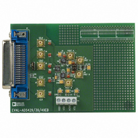
EVAL-AD5429EBZ
Manufacturer Part Number
EVAL-AD5429EBZ
Description
BOARD EVALUATION FOR AD5429
Manufacturer
Analog Devices Inc
Specifications of EVAL-AD5429EBZ
Number Of Dac's
2
Number Of Bits
8
Outputs And Type
2, Single Ended
Sampling Rate (per Second)
2.47M
Data Interface
Serial
Settling Time
30ns
Dac Type
Current
Voltage Supply Source
Single
Operating Temperature
-40°C ~ 125°C
Utilized Ic / Part
AD5429
Lead Free Status / RoHS Status
Lead free / RoHS Compliant


THEORY OF OPERATION
DIGITAL-TO-ANALOG CONVERTER
The AD5429/AD5439/AD5449 are 8-, 10-, and 12-bit, dual-
channel, current output DACs consisting of a standard inverting
R-2R ladder configuration. Figure 37 shows a simplified diagram
for a single channel of the AD5449. The feedback resistor, R
has a value of R. The value of R is typically 10 kΩ (with a
minimum of 8 kΩ and a maximum of 12 kΩ). If I
I
into each ladder leg, regardless of digital input code. Therefore,
the input resistance presented at V
Access is provided to the V
nals of the DACs, making the devices extremely versatile and
allowing them to be configured in several operating modes, such
as unipolar mode, bipolar output mode, or single-supply mode.
CIRCUIT OPERATION
Unipolar Mode
Using a single op amp, these devices can easily be configured to
provide 2-quadrant multiplying operation or a unipolar output
voltage swing, as shown in Figure 38.
OUT
V
2A are kept at the same potential, a constant current flows
REF
A
2R
S1
R
DAC DATA LATCHES
AND DRIVERS
2R
Figure 37. Simplified Ladder
S2
R
2R
S3
REF
x, R
R
FB
REF
x, I
A is always constant.
V
2R
S12
OUT
REF
1x, and I
NOTES
1. R1 AND R2 USED ONLY IF GAIN ADJUSTMENT IS REQUIRED.
2. C1 PHASE COMPENSATION (1pF TO 2pF) MAY BE REQUIRED
3. DAC B OMITTED FOR CLARITY.
R1
2R
IF A1 IS A HIGH SPEED AMPLIFIER.
R
MICROCONTROLLER
V
SYNC
OUT
OUT
REF
1A and
x
2x termi-
R
I
I
OUT
OUT
SCLK
FB
AD5429/
AD5439/
AD5449
A
Figure 38. Unipolar Operation
1A
2A
V
V
DD
DD
SDIN
FB
Rev. C | Page 15 of 32
A,
GND
R
FB
I
I
OUT
OUT
A
1A
2A
R2
When an output amplifier is connected in unipolar mode, the
output voltage is given by
where:
D is the fractional representation of the digital word loaded to
the DAC.
n is the number of bits.
With a fixed 10 V reference, the circuit shown in Figure 38 gives
a unipolar 0 V to −10 V output voltage swing. When V
signal, the circuit performs 2-quadrant multiplication.
Table 5 shows the relationship between digital code and the
expected output voltage for unipolar operation using the 8-bit
AD5429 DAC.
Table 5. Unipolar Code Table
Digital Input
1111 1111
1000 0000
0000 0001
0000 0000
AGND
D = 0 to 255 (AD5429)
C1
V
= 0 to 1023 (AD5439)
= 0 to 4095 (AD5449)
OUT
A1
V
=
OUT
−
V
= 0V TO –V
REF
×
D
REF
2 /
AD5429/AD5439/AD5449
Analog Output (V)
−V
−V
−V
−V
n
REF
REF
REF
REF
(128/256) = −V
(255/256)
(1/256)
(0/256) = 0
REF
/2
IN
is an ac
Related parts for EVAL-AD5429EBZ
Image
Part Number
Description
Manufacturer
Datasheet
Request
R


Part Number:
Description:
BOARD EVAL FOR SI270X-A
Manufacturer:
Silicon Laboratories Inc
Datasheet:

Part Number:
Description:
BUCK CONV REF DESIGN KIT IP1201
Manufacturer:
International Rectifier
Datasheet:
Part Number:
Description:
BOARD DEMO SYNC DUAL BUCK CNVTER
Manufacturer:
International Rectifier
Datasheet:
Part Number:
Description:
BOARD DEMO SYNC BUCK CONVETER
Manufacturer:
International Rectifier
Datasheet:

Part Number:
Description:
EVALBOARD/EB Omnidirectional microphone - Analog
Manufacturer:
Analog Devices
Datasheet:
Part Number:
Description:
EVALBOARD/EB Omnidirectional microphone - Analog
Manufacturer:
Analog Devices
Datasheet:


Part Number:
Description:
BOARD EVAL LED DRIVER LT3756
Manufacturer:
Linear Technology
Datasheet:

Part Number:
Description:
BOARD EVAL FOR AD7741/7742
Manufacturer:
Analog Devices Inc
Datasheet:

Part Number:
Description:
±1.7g Dual-Axis IMEMS Accelerometer Evaluation Board
Manufacturer:
Analog Devices Inc
Datasheet:

Part Number:
Description:
IC MULTIPLIER ANALOG 8-SOIC T/R
Manufacturer:
Analog Devices Inc
Datasheet:

Part Number:
Description:
IC ANALOG MULTIPLIER 8-DIP
Manufacturer:
Analog Devices Inc
Datasheet:
Part Number:
Description:
IC ANALOG MULTIPLIER 8-SOIC
Manufacturer:
Analog Devices Inc
Datasheet:
Part Number:
Description:
IC ANALOG MULTIPLIER 8-DIP
Manufacturer:
Analog Devices Inc
Datasheet: