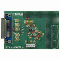
EVAL-AD5415EBZ Analog Devices Inc, EVAL-AD5415EBZ Datasheet - Page 16
EVAL-AD5415EBZ
Manufacturer Part Number
EVAL-AD5415EBZ
Description
BOARD EVALUATION FOR AD5415
Manufacturer
Analog Devices Inc
Specifications of EVAL-AD5415EBZ
Number Of Dac's
2
Number Of Bits
12
Outputs And Type
2, Differential
Sampling Rate (per Second)
2.47M
Data Interface
Serial
Settling Time
120ns
Dac Type
Current
Voltage Supply Source
Single
Operating Temperature
-40°C ~ 125°C
Utilized Ic / Part
AD5415
Lead Free Status / RoHS Status
Lead free / RoHS Compliant


AD5415
Bipolar Operation
In some applications, it may be necessary to generate full
4-quadrant multiplying operation or a bipolar output swing.
This can easily be accomplished by using another external
amplifier and the on-chip 4-quadrant resistors, as shown in
Figure 35.
When in bipolar mode, the output voltage is given by
where:
D is the fractional representation, in the range of 0 to 4,095, of
the digital word loaded to the DAC.
n is the number of bits.
When V
multiplication.
Table 6 shows the relationship between digital code and the
expected output voltage for bipolar operation.
Table 6. Bipolar Code
Digital Input
1111 1111 1111
1000 0000 0000
0000 0000 0001
0000 0000 0000
Stability
In the I-to-V configuration, the I
inverting node of the op amp must be connected as close as
possible, and proper PCB layout techniques must be used.
Because every code change corresponds to a step function, gain
peaking may occur if the op amp has limited gain bandwidth
product (GBP) and there is excessive parasitic capacitance at the
inverting node. This parasitic capacitance introduces a pole into
the open-loop response, which can cause ringing or instability
in the closed-loop applications circuit.
An optional compensation capacitor, C1, can be added in
parallel with R
Figure 35. Too small a value of C1 can produce ringing at
the output, whereas too large a value can adversely affect the
settling time. C1 should be found empirically, but 1 pF to 2 pF
is generally adequate for the compensation.
V
OUT
IN
= ( V
is an ac signal, the circuit performs 4-quadrant
REF
FB
A for stability, as shown in Figure 34 and
× D /2
n − 1
) − V
REF
Analog Output (V)
+V
0
−V
−V
OUT
REF
REF
REF
of the DAC and the
(4,095/4,096)
(4,095/4,096)
(4,096/4,096)
Rev. B | Page 16 of 32
AGND
NOTES
1. DAC B OMITTED FOR CLARITY.
2. C1 PHASE COMPENSATION (1pF TO 2pF) MAY BE REQUIRED
SINGLE-SUPPLY APPLICATIONS
Voltage-Switching Mode of Operation
Figure 36 shows the DAC operating in the voltage-switching
mode. The reference voltage, V
I
available at the V
reference voltage results in a positive output voltage, making
single-supply operation possible. The output from the DAC is
voltage at a constant impedance (the DAC ladder resistance).
Therefore, an op amp is necessary to buffer the output voltage.
The reference input no longer sees a constant input impedance,
but one that varies with code. Therefore, the voltage input
should be driven from a low impedance source.
Note that V
the DAC ladder no longer have the same source-drain drive
voltage. As a result, their on resistance differs and degrades the
integral linearity of the DAC. Also, V
more than 0.3 V, or an internal diode turns on, causing the device
to exceed the maximum ratings. In this type of application, the
full range of multiplying capability of the DAC is lost.
OUT
IF A1 IS A HIGH SPEED AMPLIFIER.
V
NOTES
1. SIMILAR CONFIGURATION FOR DACB
2. C1 PHASE COMPENSATION (1pF TO 2pF) MAY BE REQUIRED
IN
V
IF A1 IS A HIGH SPEED AMPLIFIER.
IN
2A is connected to AGND, and the output voltage is
A1
R2_3A
R2A
R3A
Figure 36. Single-Supply Voltage-Switching Mode
IN
I
I
OUT
OUT
is limited to low voltages because the switches in
2A
V
1A
V
R
DD
REF
R2
2R
R3
2R
FB
REF
R1A
A
A V
A terminal. In this configuration, a positive
Figure 35. Bipolar Operation
GND
V
DD
DD
SYNC
R1
2R
μCONTROLLER
12-BIT DAC A
AD5415
SCLK
R
V
REF
R
2R
FB
IN
SDIN
A
, is applied to the I
AGND
GND
I
I
OUT
OUT
IN
R
FB
R
1A
2A
must not go negative by
A
1
AGND
C1
R
A1
2
OUT
V
OUT
1A pin,
= –V
IN
V
TO +V
OUT
IN
Related parts for EVAL-AD5415EBZ
Image
Part Number
Description
Manufacturer
Datasheet
Request
R


Part Number:
Description:
BOARD EVAL FOR SI270X-A
Manufacturer:
Silicon Laboratories Inc
Datasheet:

Part Number:
Description:
BUCK CONV REF DESIGN KIT IP1201
Manufacturer:
International Rectifier
Datasheet:
Part Number:
Description:
BOARD DEMO SYNC DUAL BUCK CNVTER
Manufacturer:
International Rectifier
Datasheet:
Part Number:
Description:
BOARD DEMO SYNC BUCK CONVETER
Manufacturer:
International Rectifier
Datasheet:

Part Number:
Description:
EVALBOARD/EB Omnidirectional microphone - Analog
Manufacturer:
Analog Devices
Datasheet:
Part Number:
Description:
EVALBOARD/EB Omnidirectional microphone - Analog
Manufacturer:
Analog Devices
Datasheet:


Part Number:
Description:
BOARD EVAL LED DRIVER LT3756
Manufacturer:
Linear Technology
Datasheet:

Part Number:
Description:
BOARD EVAL FOR AD7741/7742
Manufacturer:
Analog Devices Inc
Datasheet:

Part Number:
Description:
±1.7g Dual-Axis IMEMS Accelerometer Evaluation Board
Manufacturer:
Analog Devices Inc
Datasheet:

Part Number:
Description:
IC MULTIPLIER ANALOG 8-SOIC T/R
Manufacturer:
Analog Devices Inc
Datasheet:

Part Number:
Description:
IC ANALOG MULTIPLIER 8-DIP
Manufacturer:
Analog Devices Inc
Datasheet:
Part Number:
Description:
IC ANALOG MULTIPLIER 8-SOIC
Manufacturer:
Analog Devices Inc
Datasheet:
Part Number:
Description:
IC ANALOG MULTIPLIER 8-DIP
Manufacturer:
Analog Devices Inc
Datasheet: