LM3423MHBKBSTEV/NOPB National Semiconductor, LM3423MHBKBSTEV/NOPB Datasheet - Page 6
LM3423MHBKBSTEV/NOPB
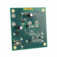
Manufacturer Part Number
LM3423MHBKBSTEV/NOPB
Description
BOARD EVAL BUCK BOOST LM3423
Manufacturer
National Semiconductor
Series
PowerWise®r
Specifications of LM3423MHBKBSTEV/NOPB
Current - Output / Channel
1A
Outputs And Type
1, Non-Isolated
Voltage - Output
35V
Features
Dimmable
Voltage - Input
4.5 ~ 35V
Utilized Ic / Part
LM3423
Lead Free Status / RoHS Status
Lead free / RoHS Compliant
Other names
LM3423MHBKBSTEV


www.national.com
DIM DRIVER (DIM, DDRV)
nDIM
nDIM
R
R
PULL-DOWN N-CHANNEL MosFETS
R
R
R
THERMAL SHUTDOWN
T
T
THERMAL RESISTANCE
θ
θ
SD
HYS
JA
JC
SRC(DDRV)
SNK(DDRV)
RPD
FLT
LRDY
Symbol
Note 1: Absolute Maximum Ratings indicate limits beyond which damage to the device may occur, including inoperability and degradation of device reliability
and/or performance. Functional operation of the device and/or non-degradation at the Absolute Maximum Ratings or other conditions beyond those indicated in
the Operating Ratings is not implied. The recommended Operating Ratings indicate conditions at which the device is functional and the device should not be
operated beyond such conditions. All voltages are with respect to the potential at the AGND pin, unless otherwise specified.
Note 2: Junction-to-ambient thermal resistance is highly board-layout dependent. The numbers listed in the table are given for an reference layout wherein the
16L TSSOP package has its EP pad populated with 9 vias and the 20L TSSOP has its EP pad populated with 12 vias. In applications where high maximum power
dissipation exists, namely driving a large MosFET at high switching frequency from a high input voltage, special care must be paid to thermal dissipation issues
during board design. In high-power dissipation applications, the maximum ambient temperature may have to be derated. Maximum ambient temperature (T
MAX
the application (P
MAX-OP
vias would be required and the thermal resistances would be 104 °C/W for the 16L TSSOP and 86.7 °C/W for the 20L TSSOP. It is possible to conservatively
interpolate between the full via count thermal resistance and the no via count thermal resistance with a straight line to get a thermal resistance for any number
of vias in between these two limits.
Note 3: Refer to National’s packaging website for more detailed information and mounting techniques. http://www.national.com/analog/packaging/
Note 4: The human body model is a 100 pF capacitor discharged through a 1.5 kΩ resistor into each pin. The applicable standard is JESD22-A114C.
Note 5: All limits guaranteed at room temperature (standard typeface) and at temperature extremes (bold typeface). All room temperature limits are 100%
production tested. All limits at temperature extremes are guaranteed via correlation using standard Statistical Quality Control (SQC) methods. All limits are used
to calculate Average Outgoing Quality Level (AOQL).
Note 6: Typical numbers are at 25°C and represent the most likely norm.
Note 7: These electrical parameters are guaranteed by design, and are not verified by test.
Note 8: The measurements were made using the standard buck-boost evaluation board from AN-2010.
Note 9: The measurements were made using the standard boost evaluation board from AN-2011.
) is dependent on the maximum operating junction temperature (T
VTH
HYS
– (θ
JA
× P
nDIM / UVLO Threshold
nDIM Hysteresis Current
DDRV Sourcing Resistance
DDRV Sinking Resistance
RPD Pull-down Resistance
FLT Pull-down Resistance
LRDY Pull-down Resistance
Thermal Shutdown Threshold
Thermal Shutdown Hysteresis
Junction to Ambient
Junction to Exposed Pad (EP) 16L TSSOP EP
D-MAX
D-MAX
). In most applications there is little need for the full power dissipation capability of this advanced package. Under these circumstances, no
), and the junction-to ambient thermal resistance of the package in the application (θ
Parameter
(Note
2)
DDRV = High
DDRV = Low
(Note
(Note
16L TSSOP EP
20L TSSOP EP
20L TSSOP EP
Conditions
7)
7)
J-MAX-OP
= 125°C for Q1, or 150°C for Q0), the maximum power dissipation of the device in
6
Range
Temp
Q1
Q0
Q1
Q0
Q1
Q0
Q1
Q0
Q1
Q0
(Note
1.185
Min
20
5)
JA
), as given by the following equation: T
(Note
1.240
13.5
37.4
34.0
Typ
145
145
135
165
210
3.5
2.3
2.3
23
25
6)
(Note
1.285
Max
30.0
10.0
300
350
300
350
300
350
25
26
5)
A-MAX
Units
°C/W
°C/W
= T
µA
°C
Ω
Ω
V
A-
J-
Related parts for LM3423MHBKBSTEV/NOPB
Image
Part Number
Description
Manufacturer
Datasheet
Request
R

Part Number:
Description:
National Semiconductor [8-Bit D/A Converter]
Manufacturer:
National Semiconductor
Datasheet:
Part Number:
Description:
National Semiconductor [Media Coprocessor]
Manufacturer:
National Semiconductor
Datasheet:
Part Number:
Description:
Digitally Controlled Tone and Volume Circuit with Stereo Audio Power Amplifier, Microphone Preamp Stage and National 3D Sound
Manufacturer:
National Semiconductor
Datasheet:
Part Number:
Description:
Digitally Controlled Tone and Volume Circuit with Stereo Audio Power Amplifier, Microphone Preamp Stage and National 3D Sound
Manufacturer:
National Semiconductor
Datasheet:
Part Number:
Description:
AC97 Rev 2 Codec with Sample Rate Conversion and National 3D Sound
Manufacturer:
National Semiconductor
Part Number:
Description:
Manufacturer:
National Semiconductor
Datasheet:
Part Number:
Description:
Manufacturer:
National Semiconductor
Datasheet:
Part Number:
Description:
General Purpose, Low Voltage, Low Power, Rail-to-Rail Output Operational Amplifiers
Manufacturer:
National Semiconductor
Datasheet:
Part Number:
Description:
8-bit 20 MSPS flash A/D converter.
Manufacturer:
National Semiconductor
Datasheet:
Part Number:
Description:
Low Noise Quad Operational Amplifier
Manufacturer:
National Semiconductor
Datasheet:
Part Number:
Description:
Quad Differential Line Receivers
Manufacturer:
National Semiconductor
Datasheet:
Part Number:
Description:
Quad High Speed Trapezoidal? Bus Transceiver
Manufacturer:
National Semiconductor
Datasheet:
Part Number:
Description:
Dual Line Receiver
Manufacturer:
National Semiconductor
Datasheet:
Part Number:
Description:
TTL to 10k ECL Level Translator with Latch
Manufacturer:
National Semiconductor
Datasheet: