NCP1351LEDGEVB ON Semiconductor, NCP1351LEDGEVB Datasheet - Page 11
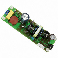
NCP1351LEDGEVB
Manufacturer Part Number
NCP1351LEDGEVB
Description
EVAL BOARD FOR NCP1351LEDG
Manufacturer
ON Semiconductor
Datasheets
1.NCP1351APG.pdf
(27 pages)
2.NCP1351LEDGEVB.pdf
(11 pages)
3.NCP1351LEDGEVB.pdf
(3 pages)
Specifications of NCP1351LEDGEVB
Design Resources
NCP1351 EVB BOM NCP1351LEDGEVB Gerber Files NCP1351LED EVB Schematic
Current - Output / Channel
700mA
Outputs And Type
1, Isolated
Voltage - Output
33V
Features
Short-Circuit Protection
Voltage - Input
85 ~ 265 V
Utilized Ic / Part
NCP1351
Core Chip
NCP1351
Topology
Flyback
No. Of Outputs
1
Output Current
700mA
Output Voltage
33V
Development Tool Type
Hardware - Eval/Demo Board
Leaded Process Compatible
Yes
Rohs Compliant
Yes
Lead Free Status / RoHS Status
Lead free / RoHS Compliant
For Use With/related Products
NCP1351LEDG
Other names
NCP1351LEDGEVBOS


The constant current constant voltage secondary control loop is very flexible and is implemented using a PNP (Q3) with a
pair of current sense resistors (R12 & R13) to regulate the current and provide control of the optocoupler to the NCP1351.
In addition, there is a maximum voltage control loop that is implemented using zener D10. To modify this circuit for
alternate current / voltage configurations, these components should be modified. The table on the front page shows
several other possible configuration options.
transformer design and FET used, as the current decreases, the maximum voltage capability increases. For example, for
20W output, the maximum voltage at 350 mA could be as high as 57 Vdc. Under UL1310, Class 2 power supplies for use
in dry/damp environments are allowed to have a maximum output voltage of 60 Vdc.
implemented using a BC857 transistor which has a maximum V
this transistor can be changed to a BC856 (maximum V
performance for a nominal 350 mA output current with the component changes as noted.
September 2008, Rev. 2
Disclaimer: ON Semiconductor is providing this design note “AS IS” and does not assume any liability arising from its use; nor
does ON Semiconductor convey any license to its or any third party’s intellectual property rights. This document is provided only to
assist customers in evaluation of the referenced circuit implementation and the recipient assumes all liability and risk associated
with its use, including, but not limited to, compliance with all regulatory standards. ON Semiconductor may change any of its
products at any time, without notice.
Design note created by Anthony Middleton, e-mail: Anthony.Middleton@onsemi.com
0.40
0.35
0.30
0.25
0.20
0.15
0.10
0.05
0.00
0
R12 & R13 = 3.6 ohms each, D10 = MMSZ5263B (56V), Q3 = BC856
5
Typical Current Regulation versus Load, T
Modifying the Board for Other LED currents
10
15
1
© 2008 ON Semiconductor.
LED Forward Voltage (Vdc)
20
Note because this design is ultimately power limited based on the
DN06040/D
www.onsemi.com
25
CEO
of -65 Vdc). The figure below shows the current regulation
30
CEO
of -45 Vdc. If a higher operating voltage is required,
35
a
= 21˚C / 70˚F
40
45
On the demo board, Q3 is
50
55
60
11
Related parts for NCP1351LEDGEVB
Image
Part Number
Description
Manufacturer
Datasheet
Request
R

Part Number:
Description:
ON Semiconductor [VOLTAGE REGULATOR]
Manufacturer:
ON Semiconductor
Datasheet:
Part Number:
Description:
357-036-542-201 CARDEDGE 36POS DL .156 BLK LOPRO
Manufacturer:
ON Semiconductor
Datasheet:
Part Number:
Description:
357-036-542-201 CARDEDGE 36POS DL .156 BLK LOPRO
Manufacturer:
ON Semiconductor
Datasheet:
Part Number:
Description:
357-036-542-201 CARDEDGE 36POS DL .156 BLK LOPRO
Manufacturer:
ON Semiconductor
Datasheet:
Part Number:
Description:
357-036-542-201 CARDEDGE 36POS DL .156 BLK LOPRO
Manufacturer:
ON Semiconductor
Datasheet:
Part Number:
Description:
357-036-542-201 CARDEDGE 36POS DL .156 BLK LOPRO
Manufacturer:
ON Semiconductor
Datasheet:
Part Number:
Description:
357-036-542-201 CARDEDGE 36POS DL .156 BLK LOPRO
Manufacturer:
ON Semiconductor
Datasheet:
Part Number:
Description:
357-036-542-201 CARDEDGE 36POS DL .156 BLK LOPRO
Manufacturer:
ON Semiconductor
Datasheet:
Part Number:
Description:
357-036-542-201 CARDEDGE 36POS DL .156 BLK LOPRO
Manufacturer:
ON Semiconductor
Datasheet:
Part Number:
Description:
357-036-542-201 CARDEDGE 36POS DL .156 BLK LOPRO
Manufacturer:
ON Semiconductor
Datasheet:
Part Number:
Description:
357-036-542-201 CARDEDGE 36POS DL .156 BLK LOPRO
Manufacturer:
ON Semiconductor
Datasheet:
Part Number:
Description:
Manufacturer:
ON Semiconductor
Datasheet:
Part Number:
Description:
Manufacturer:
ON Semiconductor
Datasheet:
Part Number:
Description:
Manufacturer:
ON Semiconductor
Datasheet: