NCP1351LEDGEVB ON Semiconductor, NCP1351LEDGEVB Datasheet - Page 5
NCP1351LEDGEVB
Manufacturer Part Number
NCP1351LEDGEVB
Description
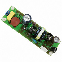
EVAL BOARD FOR NCP1351LEDG
Manufacturer
ON Semiconductor
Datasheets
1.NCP1351APG.pdf
(27 pages)
2.NCP1351LEDGEVB.pdf
(11 pages)
3.NCP1351LEDGEVB.pdf
(3 pages)
Specifications of NCP1351LEDGEVB
Design Resources
NCP1351 EVB BOM NCP1351LEDGEVB Gerber Files NCP1351LED EVB Schematic
Current - Output / Channel
700mA
Outputs And Type
1, Isolated
Voltage - Output
33V
Features
Short-Circuit Protection
Voltage - Input
85 ~ 265 V
Utilized Ic / Part
NCP1351
Core Chip
NCP1351
Topology
Flyback
No. Of Outputs
1
Output Current
700mA
Output Voltage
33V
Development Tool Type
Hardware - Eval/Demo Board
Leaded Process Compatible
Yes
Rohs Compliant
Yes
Lead Free Status / RoHS Status
Lead free / RoHS Compliant
For Use With/related Products
NCP1351LEDG
Other names
NCP1351LEDGEVBOS


Rectifier snubber
rectifier as there was a large amount of ringing present
after the rectifier turns off.
series, and knowing the junction capacitance and ringing
frequency we can determine the necessary values:
allows us to calculate the necessary snubber resistor.
...............................................................................(Eq.22)
September 2008, Rev. 2
Testing demonstrated the need for snubbing on the
The snubber consists of a resistor and capacitor in
Knowing that:
We can determine L, the stray inductance which then
C
R =
L
f
s
s
=
=
=
f = 14.5 MHz (measured on oscilloscope)
C
=
. 1
4
2
j
C
π
= 80 pF (datasheet figure for MUR840 at 62 V)
2
51
C
π
L
j
1
( )
1
j
μ
π
R
LC
H
f
.......................................................(Eq.19)
LC
s
2
j
j
=
................................................(Eq.21)
..............................................(Eq.20)
4
×
80
×
10
−
12
×
1
(
π
×
14
5 .
×
10
6
)
2
DN06040/D
www.onsemi.com
inserting these into the circuit eliminated the ringing due to
the rectifier.
Auxiliary winding
would be in the form of a flyback winding, i.e. in phase
with the output winding, and thus provide a semi-regulated
voltage to supply the controller. As this ballast is current
controlled and the output voltage can vary over a
considerable range depending on the number of LED’s
connected, a forward phased winding is used. The
auxiliary will therefore vary with line rather than output
voltage. Since neither option could supply sufficient volts
at low input/output voltage whilst still staying below the
maximum V
formed by Q1 and D6. Below ~20 V the regulator does
nothing other than act as a small volt drop, however as the
voltage rises it clamps the voltage to around 20.7 V, since
the current is very low into the V
loss.
.............................................................................. (Eq.24)
The nearest standard values are 470 pF and 140 Ω,
Normally in a flyback converter the auxiliary winding
C
R
s
s
=
=
2
. 1
×
80
CC
π
51
×
figure of 28 V, a voltage regulator is used
×
×
10
10
. 1
−
12
−
51
6
×
=
137
10
137
−
6
Ω
×
80
......................... (Eq.23)
CC
×
pin there is very little
10
−
12
=
504
pF
5
Related parts for NCP1351LEDGEVB
Image
Part Number
Description
Manufacturer
Datasheet
Request
R

Part Number:
Description:
ON Semiconductor [VOLTAGE REGULATOR]
Manufacturer:
ON Semiconductor
Datasheet:
Part Number:
Description:
357-036-542-201 CARDEDGE 36POS DL .156 BLK LOPRO
Manufacturer:
ON Semiconductor
Datasheet:
Part Number:
Description:
357-036-542-201 CARDEDGE 36POS DL .156 BLK LOPRO
Manufacturer:
ON Semiconductor
Datasheet:
Part Number:
Description:
357-036-542-201 CARDEDGE 36POS DL .156 BLK LOPRO
Manufacturer:
ON Semiconductor
Datasheet:
Part Number:
Description:
357-036-542-201 CARDEDGE 36POS DL .156 BLK LOPRO
Manufacturer:
ON Semiconductor
Datasheet:
Part Number:
Description:
357-036-542-201 CARDEDGE 36POS DL .156 BLK LOPRO
Manufacturer:
ON Semiconductor
Datasheet:
Part Number:
Description:
357-036-542-201 CARDEDGE 36POS DL .156 BLK LOPRO
Manufacturer:
ON Semiconductor
Datasheet:
Part Number:
Description:
357-036-542-201 CARDEDGE 36POS DL .156 BLK LOPRO
Manufacturer:
ON Semiconductor
Datasheet:
Part Number:
Description:
357-036-542-201 CARDEDGE 36POS DL .156 BLK LOPRO
Manufacturer:
ON Semiconductor
Datasheet:
Part Number:
Description:
357-036-542-201 CARDEDGE 36POS DL .156 BLK LOPRO
Manufacturer:
ON Semiconductor
Datasheet:
Part Number:
Description:
357-036-542-201 CARDEDGE 36POS DL .156 BLK LOPRO
Manufacturer:
ON Semiconductor
Datasheet:
Part Number:
Description:
Manufacturer:
ON Semiconductor
Datasheet:
Part Number:
Description:
Manufacturer:
ON Semiconductor
Datasheet:
Part Number:
Description:
Manufacturer:
ON Semiconductor
Datasheet: