MCP6V01DM-VOS Microchip Technology, MCP6V01DM-VOS Datasheet - Page 14
MCP6V01DM-VOS
Manufacturer Part Number
MCP6V01DM-VOS
Description
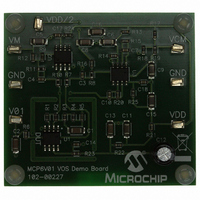
DEMO BOARD FOR MCP6V01
Manufacturer
Microchip Technology
Specifications of MCP6V01DM-VOS
Channels Per Ic
1 - Single
Amplifier Type
Chopper (Zero-Drift)
Output Type
Rail-to-Rail
Slew Rate
0.5 V/µs
Current - Output / Channel
22mA
Operating Temperature
-40°C ~ 125°C
Voltage - Supply, Single/dual (±)
1.8 V ~ 5.5 V
Board Type
Fully Populated
Utilized Ic / Part
MCP6V01
Silicon Manufacturer
Microchip
Application Sub Type
Operational Amplifier
Kit Application Type
Amplifier
Silicon Core Number
MCP6V01, MCP6V03, MCP6V06, MCP6V08
Kit Contents
Board
Lead Free Status / RoHS Status
Lead free / RoHS Compliant
-3db Bandwidth
-
Current - Supply (main Ic)
-
Lead Free Status / Rohs Status
Lead free / RoHS Compliant


MCP6V01 Input Offset Demo Board User’s Guide
2.4
2.5
2.6
DS51801A-page 10
OPERATING CONDITIONS
CALCULATING THE DUT’S INPUT OFFSET VOLTAGE
CONVERTING INPUT OFFSET VOLTAGE TO OTHER PARAMETERS
This board works most effectively at room temperature (near +25°C). Measurements
at other temperatures should be done in an oven where the air velocity is minimal.
The power supply (V
The common mode voltage (V
operation of this demo board.
The DUT’s total input offset voltage (V
shown in Equation 2-1.
EQUATION 2-1:
2.6.1
Changing the bias voltages changes the input offset voltage. Microchip’s application
note AN1177 discusses in detail how these changes in V
found in our data sheets. The following list summarizes the parameters that contribute
to V
• Specified Input Offset Voltage:
• DC Common Mode Rejection Ratio:
• DC Power Supply Rejection Ratio:
• DC Open-Loop Gain:
• Input Offset Drift over Temperature:
V
- V
- CMRR = ΔV
- PSRR = (ΔV
- A
- ΔV
OST
Note:
Where:
OST
1/(G
OS
OL
=
OS
:
= ΔV
(
DA
= Input offset at the specified bias point
/ΔT
V
Theory
The data sheet Input Offset Voltage (V
point and temperature only. The total input offset voltage (V
V
change.
G
M
OS
N
A
–
OUT
) ≈ 10.0 µV/V
V
and other changes in input offset as bias voltages and temperature
DD
CM
DD
/ΔV
2 ⁄
/ΔV
– ΔV
DD
OS
)
⋅
OS
) should be between 1.8V and 5.5V.
(
1
SS
⁄
(
)/ΔV
G
DA
CM
OS
G
) needs to be between 0.3V and V
N
)
)
OST
) can be calculated from a measurement as
OS
) specification applies to one bias
OS
are related to specifications
© 2009 Microchip Technology Inc.
DD
– 0.3V for proper
OST
) includes
Related parts for MCP6V01DM-VOS
Image
Part Number
Description
Manufacturer
Datasheet
Request
R

Part Number:
Description:
IC OPAMP AUTO-ZERO SNGL 8SOIC
Manufacturer:
Microchip Technology
Datasheet:

Part Number:
Description:
300 ?A, Auto-Zeroed Op Amps
Manufacturer:
MICROCHIP [Microchip Technology]
Datasheet:
Part Number:
Description:
Op Amps Sngl Auto-Zero Op Amp E temp
Manufacturer:
Microchip Technology

Part Number:
Description:
300 ?a, Auto-zeroed Op Amps
Manufacturer:
Microchip Technology Inc.
Datasheet:
Part Number:
Description:
Manufacturer:
Microchip Technology Inc.
Datasheet:
Part Number:
Description:
Manufacturer:
Microchip Technology Inc.
Datasheet:
Part Number:
Description:
Manufacturer:
Microchip Technology Inc.
Datasheet:
Part Number:
Description:
Manufacturer:
Microchip Technology Inc.
Datasheet:
Part Number:
Description:
Manufacturer:
Microchip Technology Inc.
Datasheet:
Part Number:
Description:
Manufacturer:
Microchip Technology Inc.
Datasheet:
Part Number:
Description:
Manufacturer:
Microchip Technology Inc.
Datasheet: