QSK-62P PLUS BNS Solutions, QSK-62P PLUS Datasheet - Page 4
QSK-62P PLUS
Manufacturer Part Number
QSK-62P PLUS
Description
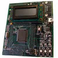
KIT QUICK START RENESAS 62P
Manufacturer
BNS Solutions
Series
M16C™r
Type
MCUr
Datasheet
1.QSK-62P_PLUS.pdf
(103 pages)
Specifications of QSK-62P PLUS
Contents
Board, Cable, CD
For Use With/related Products
M16C/62P
Lead Free Status / RoHS Status
Not applicable / Not applicable
Other names
867-1000
QSK-62P
QSK26A
QSK62P
QSK-62P
QSK26A
QSK62P


M16C/62P Group (M16C/62P, M16C/62PT)
Rev.2.41
REJ03B0001-0241
1.2
Table 1.1
NOTES:
CPU
Peripheral
Function
Electric
Characteristics
Flash memory
version
Operating Ambient Temperature
Package
Table 1.1 to 1.3 list Performance Outline of M16C/62P Group (M16C/62P, M16C/62PT)(128-pin version).
1. I
2. IEBus is a registered trademark of NEC Electronics Corporation.
3. See Table 1.8 Product Code for the program and erase endurance, and operating ambient temperature.
4. All options are on request basis.
In addition 1,000 times/10,000 times are under development as of Jul., 2005. Please inquire about a release
schedule.
2
Performance Outline
C bus is a registered trademark of Koninklijke Philips Electronics N. V.
Jan 10, 2006
Performance Outline of M16C/62P Group (M16C/62P, M16C/62PT)(128-pin version)
Number of Basic Instructions
Minimum Instruction Execution
Time
Operating Mode
Address Space
Memory Capacity
Port
Multifunction Timer
Serial Interface
A/D Converter
D/A Converter
DMAC
CRC Calculation Circuit
Watchdog Timer
Interrupt
Clock Generation Circuit
Oscillation Stop Detection
Function
Voltage Detection Circuit
Supply Voltage
Power Consumption
Program/Erase Supply Voltage
Program and Erase Endurance
Page 2 of 96
Item
91 instructions
41.7ns(f(BCLK)=24MHz, VCC1=3.3 to 5.5V)
100ns(f(BCLK)=10MHz, VCC1=2.7 to 5.5V)
Single-chip, memory expansion and microprocessor mode
1 Mbyte (Available to 4 Mbytes by memory space expansion
function)
See Table 1.4 to 1.5 Product List
Input/Output : 113 pins, Input : 1 pin
Timer A : 16 bits x 5 channels,
Timer B : 16 bits x 6 channels,
Three phase motor control circuit
3 channels
2 channels
10-bit A/D converter: 1 circuit, 26 channels
8 bits x 2 channels
2 channels
CCITT-CRC
15 bits x 1 channel (with prescaler)
Internal: 29 sources, External: 8 sources, Software: 4 sources,
Priority level: 7 levels
4 circuits
(*)Equipped with a built-in feedback resistor.
Stop detection of main clock oscillation, re-oscillation detection
function
Available (option
VCC1=3.0 to 5.5 V, VCC2=2.7V to VCC1 (f(BCLK=24MHz)
VCC1=2.7 to 5.5 V, VCC2=2.7V to VCC1 (f(BCLK=10MHz)
14 mA (VCC1=VCC2=5V, f(BCLK)=24MHz)
8 mA (VCC1=VCC2=3V, f(BCLK)=10MHz)
1.8µA (VCC1=VCC2=3V, f(XCIN)=32kHz, wait mode)
0.7µA (VCC1=VCC2=3V, stop mode)
3.3±0.3 V or 5.0±0.5 V
100 times (all area)
or 1,000 times (user ROM area without block A and block 1)
/ 10,000 times (block A, block 1)
-20 to 85°C,
-40 to 85°C
128-pin plastic mold LQFP
Clock synchronous, UART, I
Clock synchronous
Main clock generation circuit (*),
Subclock generation circuit (*),
On-chip oscillator, PLL synthesizer
(3)
(4)
)
Performance
M16C/62P
2
C bus
(3)
(1)
, IEBus
(2)
1. Overview