P0037 Terasic Technologies Inc, P0037 Datasheet - Page 9
P0037
Manufacturer Part Number
P0037
Description
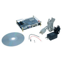
BOARD DEV/EDUCATION ALTERA DE0
Manufacturer
Terasic Technologies Inc
Type
FPGAr
Datasheet
1.EP3C5F256C8N.pdf
(34 pages)
Specifications of P0037
Contents
Board, Cable, CD, Power Supply
For Use With/related Products
Cyclone III
Lead Free Status / RoHS Status
Lead free / RoHS Compliant


Chapter 1: Cyclone III Device Data Sheet
Electrical Characteristics
© January 2010 Altera Corporation
Example 1–1
from 25°C at 3.0 V to 85°C at 3.15 V:
Example 1–1.
Because ΔR
Because ΔR
Pin Capacitance
Table 1–9
Table 1–9. Cyclone III Devices Pin Capacitance
C
C
C
C
C
C
C
Notes to
(1) When VREF pin is used as regular input or output, a reduced performance of toggle rate and t
(2) C
Symbol
IOTB
IOLR
LV DSLR
V REFLR
V REFTB
C LKTB
C LKLR
MF
MF
MF = 0.963 × 1.157 = 1.114
R
higher pin capacitance.
VREFTB
final
ΔR
ΔR
(1)
(1)
V
T
Table
= 15.72/100 + 1 = 1.157
= 1 / (3.83/100 + 1) = 0.963
= 50 × 1.114 = 55.71 Ω
V
T
= (3.15 – 3) × 1000 × –0.026 = –3.83
= (85 – 25) × 0.262 = 15.72
for EP3C25 is 30 pF.
lists the pin capacitance for Cyclone III devices.
V
T
Input capacitance on top/bottom I/O pins
Input capacitance on left/right I/O pins
Input capacitance on left/right I/O pins with dedicated
LVDS output
Input capacitance on left/right dual-purpose VREF pin
when used as V
Input capacitance on top/bottom dual-purpose VREF pin
when used as V
Input capacitance on top/bottom dedicated clock input
pins
Input capacitance on left/right dedicated clock input pins
is negative,
is positive,
1–9:
shows you the example to calculate the change of 50 Ω I/O impedance
REF
REF
or user I/O pin
or user I/O pin
Parameter
Cyclone III Device Handbook, Volume 2
Typical –
23
QFP
21
7
8
7
6
7
(2)
Typical –
C O
23
FBGA
is expected due to
21
6
5
7
6
5
(2)
Unit
pF
pF
pF
pF
pF
pF
pF
1–9
Related parts for P0037
Image
Part Number
Description
Manufacturer
Datasheet
Request
R

Part Number:
Description:
MODULE DIGITAL CAMERA 5MP (D5M)
Manufacturer:
Terasic Technologies Inc
Datasheet:

Part Number:
Description:
DE2-70 CALL FOR ACADEMIC PRICING
Manufacturer:
Terasic Technologies Inc
Datasheet:

Part Number:
Description:
USB BLASTER CABLE
Manufacturer:
Terasic Technologies Inc
Datasheet:

Part Number:
Description:
BOARD ADAPTER HSMC TO GPIO
Manufacturer:
Terasic Technologies Inc
Datasheet:

Part Number:
Description:
BOARD ADAPTER THDB-SUM
Manufacturer:
Terasic Technologies Inc
Datasheet:

Part Number:
Description:
KIT DEV 4.3" LCD TOUCH PANEL
Manufacturer:
Terasic Technologies Inc
Datasheet:

Part Number:
Description:
DAUGHTER BOARD AD/DA GPIO ADA
Manufacturer:
Terasic Technologies Inc

Part Number:
Description:
DAUGHTER BOARD AD/DA HSMC ADA
Manufacturer:
Terasic Technologies Inc

Part Number:
Description:
KIT MAX II MICRO
Manufacturer:
Terasic Technologies Inc
Datasheet:

Part Number:
Description:
BOARD DEV DE1 ALTERA
Manufacturer:
Terasic Technologies Inc
Datasheet:

Part Number:
Description:
DE2 CALL FOR ACADEMIC PRICING
Manufacturer:
Terasic Technologies Inc

Part Number:
Description:
MODULE DIGITAL CAMERA 1.3MP
Manufacturer:
Terasic Technologies Inc
Datasheet:

Part Number:
Description:
SENSOR CMOS 1.3MEGA (FOR P0349)
Manufacturer:
Terasic Technologies Inc
Datasheet:
Part Number:
Description:
MODULE DIGITAL CAMERA 5MP (D5M)
Manufacturer:
Terasic Technologies Inc
Datasheet: