DK-MAXII-1270N Altera, DK-MAXII-1270N Datasheet - Page 16
DK-MAXII-1270N
Manufacturer Part Number
DK-MAXII-1270N
Description
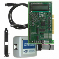
KIT DEV MAXII W/EPM 1270N
Manufacturer
Altera
Series
MAX® IIr
Type
CPLDr
Specifications of DK-MAXII-1270N
Contents
Dev Board, Quartus®II Web Edition, Nios®II Web Edition, Cables, Accessories, Reference Designs and Demos
Silicon Manufacturer
Altera
Core Architecture
CPLD
Core Sub-architecture
MAX
Silicon Core Number
EPM
Silicon Family Name
MAX II
Rohs Compliant
Yes
For Use With/related Products
MAX®II CPLDs
Lead Free Status / RoHS Status
Lead free / RoHS Compliant
Other names
544-2380
Available stocks
Company
Part Number
Manufacturer
Quantity
Price


Demo Designs
2–8
MAX II Development Kit Getting Started User Guide
w
Before performing a test to verify the power-up time of a MAX II device
under a certain load, you should set the V
depending on what it will be in the final system. The shunt on J9 controls
this value. If the shunt is present on J9, the MAX II device’s V
2.5 V; if the shunt is not present on J9, the V
The MAX II device data sheet specifies that a MAX II device will be
functional less than 300 μs after minimum V
actuality, configuration starts at a voltage below minimum V
device on a board where the V
powered-up and configured before the supply reaches minimum V
The Power-up demo allows users to investigate the power-up time in two
different ways. The first is a race against the MAX II device that helps
define what “Instant-on” means. The second is a much more detailed
investigation of the power-up time that requires an oscilloscope, but
provides a thorough understanding of how a MAX II device powers up
under different loads.
On Board Circuit
The circuit on the board consists of a power regulator that provides the
V
or removing a shunt on J9. (If the shunt is in place, V
shunt is not in place, V
increased by a variable resistor (POT1). Four test points are also provided
on the board: V
test points are labeled Active I/O Test Points and are located near the
prototyping area on the board. Refer to the MAX II Development Board
Data Sheet if you cannot locate the test points on your board. These test
points allow for oscilloscope probes to be attached so the outputs can be
thoroughly examined.
CCINT
voltage. The power regulator can be set to 2.5 V or 3.3 V by adding
Development Kit Version 1.1.0
This test is meant to verify the data provided in the MAX II
Device Data Sheet, not to replace it. All MAX II devices will have
some fluctuation in power-up timing. Designers should ensure
that systems relying on a MAX II device to perform power up
functions are using the MAX II device in accordance with the
specifications given in the Data Sheet.
CCINT
, V
CCIO
CCINT
, GND, and a MAX II User I/O pin. These four
= 3.3 V.) The load on the regulator can be
CC
rise time is greater than 1 ms will be fully
CCINT
CCINT
CC
level is reached. In
supply to 2.5 V or 3.3 V,
value is 3.3 V.
CCINT
Altera Corporation
= 2.5 V; if the
CC
CCINT
. A MAX II
July 2005
is
CC
.
Related parts for DK-MAXII-1270N
Image
Part Number
Description
Manufacturer
Datasheet
Request
R

Part Number:
Description:
KIT DEV MAX V 5M570Z
Manufacturer:
Altera
Datasheet:

Part Number:
Description:
CYCLONE II STARTER KIT EP2C20N
Manufacturer:
Altera
Datasheet:


Part Number:
Description:
CPLD, EP610 Family, ECMOS Process, 300 Gates, 16 Macro Cells, 16 Reg., 16 User I/Os, 5V Supply, 35 Speed Grade, 24DIP
Manufacturer:
Altera Corporation
Datasheet:
Part Number:
Description:
CPLD, EP610 Family, ECMOS Process, 300 Gates, 16 Macro Cells, 16 Reg., 16 User I/Os, 5V Supply, 15 Speed Grade, 24DIP
Manufacturer:
Altera Corporation
Datasheet:
Part Number:
Description:
Manufacturer:
Altera Corporation
Datasheet:
Part Number:
Description:
CPLD, EP610 Family, ECMOS Process, 300 Gates, 16 Macro Cells, 16 Reg., 16 User I/Os, 5V Supply, 30 Speed Grade, 24DIP
Manufacturer:
Altera Corporation
Datasheet:
Part Number:
Description:
High-performance, low-power erasable programmable logic devices with 8 macrocells, 10ns
Manufacturer:
Altera Corporation
Datasheet:
Part Number:
Description:
High-performance, low-power erasable programmable logic devices with 8 macrocells, 7ns
Manufacturer:
Altera Corporation
Datasheet:
Part Number:
Description:
Classic EPLD
Manufacturer:
Altera Corporation
Datasheet:
Part Number:
Description:
High-performance, low-power erasable programmable logic devices with 8 macrocells, 10ns
Manufacturer:
Altera Corporation
Datasheet:
Part Number:
Description:
Manufacturer:
Altera Corporation
Datasheet:
Part Number:
Description:
Manufacturer:
Altera Corporation
Datasheet:
Part Number:
Description:
Manufacturer:
Altera Corporation
Datasheet: