EVAL-ADUC841QSZ Analog Devices Inc, EVAL-ADUC841QSZ Datasheet - Page 3
EVAL-ADUC841QSZ
Manufacturer Part Number
EVAL-ADUC841QSZ
Description
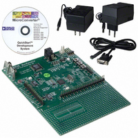
KIT DEV FOR ADUC841 QUICK START
Manufacturer
Analog Devices Inc
Series
QuickStart™ Kitr
Type
MCUr
Specifications of EVAL-ADUC841QSZ
Contents
Evaluation Board, Power Supply, Cable, Software and Documentation
Silicon Manufacturer
Analog Devices
Core Architecture
8052
Silicon Core Number
ADUC841
Tool / Board Applications
General Purpose MCU, MPU, DSP, DSC
Mcu Supported Families
ADUC8xx
Development Tool Type
Hardware - Eval/Demo Board
Rohs Compliant
Yes
Lead Free Status / RoHS Status
Lead free / RoHS Compliant
For Use With/related Products
ADuC841
Lead Free Status / Rohs Status
Compliant
Other names
EVAL-ADUC841QS
EVAL-ADUC841QS
EVAL-ADUC841QS


SPECIFICATIONS
Table 1. AV
all specifications T
Parameter
ADC CHANNEL SPECIFICATIONS
DC ACCURACY
CALIBRATED ENDPOINT ERRORS
DYNAMIC PERFORMANCE
ANALOG INPUT
TEMPERATURE SENSOR
DAC CHANNEL SPECIFICATIONS
Internal Buffer Enabled
ADuC841/ADuC842 Only
DC ACCURACY
ANALOG OUTPUTS
Resolution
Integral Nonlinearity
Differential Nonlinearity
Integral Nonlinearity
Differential Nonlinearity
Code Distribution
Offset Error
Offset Error Match
Gain Error
Gain Error Match
Signal-to-Noise Ratio (SNR)
Total Harmonic Distortion (THD)
Peak Harmonic or Spurious Noise
Channel-to-Channel Crosstalk
Input Voltage Range
Leakage Current
Input Capacitance
Voltage Output at 25°C
Voltage TC
Accuracy
Resolution
Relative Accuracy
Differential Nonlinearity
Offset Error
Gain Error
Gain Error Mismatch
Voltage Range_0
Voltage Range_1
Output Impedance
DD
2, 3
10
= DV
A
DD
= T
= 2.7 V to 3.6 V or 4.75 V to 5.25 V; V
9
4
MIN
1
to T
4
11
7
5, 6
MAX
8
, unless otherwise noted
V
±1
±0.3
+1/–0.9
±0.3
±2
+1.5/–0.9
1
±3
±1
±3
±1
71
–85
–80
±1
–1.4
±1.5
±3
–1
±1/2
±50
±1
±1
12
–85
0 to V
32
700
12
0.5
0 to V
0 to V
0.5
DD
= 5 V
REF
REF
DD
Rev. 0 | Page 3 of 88
V
12
±1
±0.3
+1/–0.9
±0.3
±1.5
+1.5/–0.9
1
±2
±1
±2
±1
71
–85
–85
–80
0 to V
±1
32
700
–1.4
±1.5
12
±3
–1
±1/2
±50
±1
±1
0.5
0 to V
0 to V
0.5
REF
DD
= 2.5 V internal reference, f
= 3 V
REF
REF
DD
Unit
Bits
LSB max
LSB typ
LSB max
LSB typ
LSB max
LSB max
LSB typ
LSB max
LSB typ
LSB max
LSB typ
dB typ
dB typ
dB typ
dB typ
V
µA max
pF typ
mV typ
mV/°C typ
°C typ
Bits
LSB typ
LSB max
LSB typ
mV max
% max
% typ
% typ
V typ
V typ
Ω typ
Test Conditions/Comments
f
Performance Characteristics for typical
performance at other values of f
2.5 V internal reference
2.5 V internal reference
1 V external reference
1 V external reference
ADC input is a dc voltage
f
f
Internal/External 2.5 V V
DAC load to AGND
R
Guaranteed 12-bit monotonic
V
AV
V
% of full-scale on DAC1
DAC V
DAC V
CORE
ADuC841/ADuC842/ADuC843
SAMPLE
IN
SAMPLE
L
REF
REF
= 10 kHz sine wave
= 10 kΩ, C
DD
range
range
= 16.78 MHz @ 5 V 8.38 MHz @ 3 V;
range
= 120 kHz, see the Typical
= 120 kHz
REF
REF
= 2.5 V
= V
DD
L
= 100 pF
REF
SAMPLE
Related parts for EVAL-ADUC841QSZ
Image
Part Number
Description
Manufacturer
Datasheet
Request
R


Part Number:
Description:
BOARD EVAL FOR SI270X-A
Manufacturer:
Silicon Laboratories Inc
Datasheet:

Part Number:
Description:
BUCK CONV REF DESIGN KIT IP1201
Manufacturer:
International Rectifier
Datasheet:
Part Number:
Description:
BOARD DEMO SYNC DUAL BUCK CNVTER
Manufacturer:
International Rectifier
Datasheet:
Part Number:
Description:
BOARD DEMO SYNC BUCK CONVETER
Manufacturer:
International Rectifier
Datasheet:

Part Number:
Description:
EVALBOARD/EB Omnidirectional microphone - Analog
Manufacturer:
Analog Devices
Datasheet:
Part Number:
Description:
EVALBOARD/EB Omnidirectional microphone - Analog
Manufacturer:
Analog Devices
Datasheet:


Part Number:
Description:
BOARD EVAL LED DRIVER LT3756
Manufacturer:
Linear Technology
Datasheet:

Part Number:
Description:
BOARD EVAL FOR AD7741/7742
Manufacturer:
Analog Devices Inc
Datasheet:

Part Number:
Description:
±1.7g Dual-Axis IMEMS Accelerometer Evaluation Board
Manufacturer:
Analog Devices Inc
Datasheet:

Part Number:
Description:
IC MULTIPLIER ANALOG 8-SOIC T/R
Manufacturer:
Analog Devices Inc
Datasheet:

Part Number:
Description:
IC ANALOG MULTIPLIER 8-DIP
Manufacturer:
Analog Devices Inc
Datasheet:
Part Number:
Description:
IC ANALOG MULTIPLIER 8-SOIC
Manufacturer:
Analog Devices Inc
Datasheet:
Part Number:
Description:
IC ANALOG MULTIPLIER 8-DIP
Manufacturer:
Analog Devices Inc
Datasheet: