EVAL-ADUC847QSZ Analog Devices Inc, EVAL-ADUC847QSZ Datasheet - Page 10
EVAL-ADUC847QSZ
Manufacturer Part Number
EVAL-ADUC847QSZ
Description
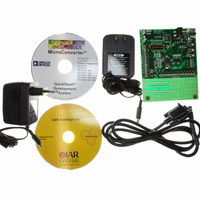
KIT DEV QUICK START FOR ADUC847
Manufacturer
Analog Devices Inc
Series
QuickStart™ Kitr
Type
MCUr
Datasheet
1.EVAL-ADUC845QSZ.pdf
(108 pages)
Specifications of EVAL-ADUC847QSZ
Contents
Evaluation Board, Power Supply, Cable, Software and Documentation
Silicon Manufacturer
Analog Devices
Core Architecture
8051
Silicon Core Number
ADuC847
Tool / Board Applications
General Purpose MCU, MPU, DSP, DSC
Mcu Supported Families
ADUC8xx
Development Tool Type
Hardware - Eval/Demo Board
Rohs Compliant
Yes
Lead Free Status / RoHS Status
Lead free / RoHS Compliant
For Use With/related Products
ADuC847
Lead Free Status / RoHS Status
Lead free / RoHS Compliant, Lead free / RoHS Compliant


ADuC845/ADuC847/ADuC848
ABOSOLUTE MAXIMUM RATINGS
T
Table 2.
Parameter
AV
AV
DV
DV
AGND to DGND
AV
Analog Input Voltage to AGND
Reference Input Voltage to AGND
AIN/REFIN Current (Indefinite)
Digital Input Voltage to DGND
Digital Output Voltage to DGND
Operating Temperature Range
Storage Temperature Range
Junction Temperature
θ
θ
Lead Temperature, Soldering
________________________
1
2
ESD CAUTION
ESD (electrostatic discharge) sensitive device. Electrostatic charges as high as 4000 V readily accumulate on
the human body and test equipment and can discharge without detection. Although this product features
proprietary ESD protection circuitry, permanent damage may occur on devices subjected to high energy
electrostatic discharges. Therefore, proper ESD precautions are recommended to avoid performance
degradation or loss of functionality.
AGND and DGND are shorted internally on the ADuC845, ADuC847, and ADuC848.
Applies to the P1.0 to P1.7 pins operating in analog or digital input modes.
JA
JA
A
Vapor Phase (60 sec)
Infrared (15 sec)
DD
DD
DD
DD
DD
= 25°C, unless otherwise noted.
Thermal Impedance (MQFP)
Thermal Impedance (LFCSP)
to AGND
to DGND
to DV
to DGND
to DGND
DD
1
2
Rating
–0.3 V to +7 V
–0.3 V to +7 V
–0.3 V to +7 V
–0.3 V to +7 V
–0.3 V to +0.3 V
–2 V to +5 V
–0.3 V to AV
–0.3 V to AV
30 mA
–0.3 V to DV
–0.3 V to DV
–40°C to +125°C
–65°C to +150°C
150°C
90°C/W
52°C/W
215°C
220°C
DD
DD
DD
DD
+ 0.3 V
+ 0.3 V
+ 0.3 V
+ 0.3 V
Rev. B | Page 10 of 108
Stresses above those listed under Absolute Maximum Ratings
may cause permanent damage to the device. This is a stress
rating only; functional operation of the device at these or any
other conditions above those listed in the operational sections
of this specification is not implied. Exposure to absolute
maximum rating conditions for extended periods may affect
device reliability.
Related parts for EVAL-ADUC847QSZ
Image
Part Number
Description
Manufacturer
Datasheet
Request
R


Part Number:
Description:
BOARD EVAL FOR SI270X-A
Manufacturer:
Silicon Laboratories Inc
Datasheet:

Part Number:
Description:
BUCK CONV REF DESIGN KIT IP1201
Manufacturer:
International Rectifier
Datasheet:
Part Number:
Description:
BOARD DEMO SYNC DUAL BUCK CNVTER
Manufacturer:
International Rectifier
Datasheet:
Part Number:
Description:
BOARD DEMO SYNC BUCK CONVETER
Manufacturer:
International Rectifier
Datasheet:

Part Number:
Description:
EVALBOARD/EB Omnidirectional microphone - Analog
Manufacturer:
Analog Devices
Datasheet:
Part Number:
Description:
EVALBOARD/EB Omnidirectional microphone - Analog
Manufacturer:
Analog Devices
Datasheet:


Part Number:
Description:
BOARD EVAL LED DRIVER LT3756
Manufacturer:
Linear Technology
Datasheet:

Part Number:
Description:
BOARD EVAL FOR AD7741/7742
Manufacturer:
Analog Devices Inc
Datasheet:

Part Number:
Description:
±1.7g Dual-Axis IMEMS Accelerometer Evaluation Board
Manufacturer:
Analog Devices Inc
Datasheet:

Part Number:
Description:
IC MULTIPLIER ANALOG 8-SOIC T/R
Manufacturer:
Analog Devices Inc
Datasheet:

Part Number:
Description:
IC ANALOG MULTIPLIER 8-DIP
Manufacturer:
Analog Devices Inc
Datasheet:
Part Number:
Description:
IC ANALOG MULTIPLIER 8-SOIC
Manufacturer:
Analog Devices Inc
Datasheet:
Part Number:
Description:
IC ANALOG MULTIPLIER 8-DIP
Manufacturer:
Analog Devices Inc
Datasheet: