C8051F800DK Silicon Laboratories Inc, C8051F800DK Datasheet - Page 14
C8051F800DK
Manufacturer Part Number
C8051F800DK
Description
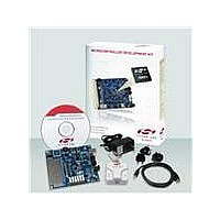
KIT DEV C8051F800
Manufacturer
Silicon Laboratories Inc
Type
MCUr
Specifications of C8051F800DK
Contents
Board, Cables, CD, Debugger, Power Supply
Processor To Be Evaluated
C8051F800
Data Bus Width
16 bit
Interface Type
USB
Operating Supply Voltage
7 V to 15 V
Lead Free Status / RoHS Status
Contains lead / RoHS non-compliant
For Use With/related Products
C8051F8xx
Lead Free Status / Rohs Status
Supplier Unconfirmed
Other names
336-1797


C8051F800-DK
7.8. Analog I/O, Voltage and Ground Reference Options (TB1, J5, J10)
Several of the C8051F800 target device’s port pins are connected to the TB1 terminal block. Refer to Table 4 for
the TB1 terminal block connections. The J5 header connects the MCU VREF pin (P0.0) to the VREF bypass
capacitors C18 and C19, and also to TB1 pin 6 for an optional external VREF input. The J10 header connects P0.1
to GND, and is useful if the P0.1/AGND option is enabled via the REF0CN register in the C8051F800. Refer to the
C8051F80x-83x data sheet for more information on configuring the voltage and ground reference options.
7.9. C2 Pin Sharing
On the C8051F800, the debug pins C2CK and C2D are shared with the pins RST and P2.0 respectively. The target
board includes the resistors necessary to enable pin sharing which allow the RST and P2.0 pins to be used
normally while simultaneously debugging the device. See Application Note “AN124: Pin Sharing Techniques for the
C2 Interface” at
14
www.silabs.com
Table 4. TB1 Terminal Block Pin Descriptions
for more information regarding pin sharing.
Pin #
1
2
3
4
5
6
P0.0/VREF (Voltage Reference)
Rev. 0.1
P0.6/CNVSTR
GND (Ground)
Description
P0.1/AGND
P1.0
P1.1
Related parts for C8051F800DK
Image
Part Number
Description
Manufacturer
Datasheet
Request
R

Part Number:
Description:
SMD/C°/SINGLE-ENDED OUTPUT SILICON OSCILLATOR
Manufacturer:
Silicon Laboratories Inc
Part Number:
Description:
Manufacturer:
Silicon Laboratories Inc
Datasheet:
Part Number:
Description:
N/A N/A/SI4010 AES KEYFOB DEMO WITH LCD RX
Manufacturer:
Silicon Laboratories Inc
Datasheet:
Part Number:
Description:
N/A N/A/SI4010 SIMPLIFIED KEY FOB DEMO WITH LED RX
Manufacturer:
Silicon Laboratories Inc
Datasheet:
Part Number:
Description:
N/A/-40 TO 85 OC/EZLINK MODULE; F930/4432 HIGH BAND (REV E/B1)
Manufacturer:
Silicon Laboratories Inc
Part Number:
Description:
EZLink Module; F930/4432 Low Band (rev e/B1)
Manufacturer:
Silicon Laboratories Inc
Part Number:
Description:
I°/4460 10 DBM RADIO TEST CARD 434 MHZ
Manufacturer:
Silicon Laboratories Inc
Part Number:
Description:
I°/4461 14 DBM RADIO TEST CARD 868 MHZ
Manufacturer:
Silicon Laboratories Inc
Part Number:
Description:
I°/4463 20 DBM RFSWITCH RADIO TEST CARD 460 MHZ
Manufacturer:
Silicon Laboratories Inc
Part Number:
Description:
I°/4463 20 DBM RADIO TEST CARD 868 MHZ
Manufacturer:
Silicon Laboratories Inc
Part Number:
Description:
I°/4463 27 DBM RADIO TEST CARD 868 MHZ
Manufacturer:
Silicon Laboratories Inc
Part Number:
Description:
I°/4463 SKYWORKS 30 DBM RADIO TEST CARD 915 MHZ
Manufacturer:
Silicon Laboratories Inc
Part Number:
Description:
N/A N/A/-40 TO 85 OC/4463 RFMD 30 DBM RADIO TEST CARD 915 MHZ
Manufacturer:
Silicon Laboratories Inc
Part Number:
Description:
I°/4463 20 DBM RADIO TEST CARD 169 MHZ
Manufacturer:
Silicon Laboratories Inc