EDK2378 Renesas Electronics America, EDK2378 Datasheet - Page 8
EDK2378
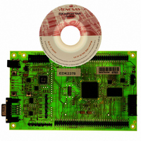
Manufacturer Part Number
EDK2378
Description
DEV EVAL KIT FOR H8S/2378
Manufacturer
Renesas Electronics America
Series
H8®r
Type
MCUr
Specifications of EDK2378
Contents
2G (Second-generation) Evaluation Board, HEW debugger support, Cable and CD-ROM
For Use With/related Products
H8S/2378
Lead Free Status / RoHS Status
Contains lead / RoHS non-compliant


4.4. M
Table 4-4 illustrates the EDK memory map for mode 4.
4.5. SRAM A
External access timing is defined by several registers, allowing different types of devices to be addressed. The registers for
the selection of wait states and signal extensions are given below with recommended values for the EDK.
Please refer to the hardware manual for the microcontroller for more information on these register settings.
4.6. LED
The EDK has four red LEDs. The function of each LED is clearly marked on the silk screen of the PCB. Please refer to the
board layout diagram for position information (Section 3).
When the board is connected to a power source the Power (PWR) led will illuminate. The Boot mode indication LED will
illuminate when the microcontroller has been placed into Boot mode. Please see section 5.7 for more details of this function.
There are two LEDs dedicated for user control these are marked USR1 and USR2. Each LED will illuminate when the port
pin is in a logical high state.
The user LEDs are connected to the following ports:
ABWCR
ASTCR
WTCRBL
RDNCR
Port C DDR
Port B DDR
Port A DDR
Port G DDR
Register
EMORY
S
M
CCESS
FEC0
FEC1
FEC5
FEC6
FE2B
FE2A
FE29
FE2F
AP
USR1
USR2
LED Identifier
H’000000
H’07FFFF
H’080000
H’0BFFFF
H’0A0000
H’1FFFFF
H’200000
H’FF3FFF
H’FF4000
H’FFBFFF
H’FFC000
H’FFCFFF
H’FFD000
H’FFFBFF
H’FFFC00
H’FFFEFF
H’FFFF00
H’FFFF1F
H’FFFF20
H’FFFFFF
Address
T
IMING
Section Start
Section End
0x00
0xFF
0x01
0x01
0xFF
0xFF
0x07
0x01
Setting for EDK
P26
P25
Recommended
Port Pin
T
ABLE
T
ABLE
Pin 57
Pin 56
Microcontroller Pin
T
4-5: SRAM A
ABLE
4-4: M
Set all 8 memory areas to be 16 bit access
Selects bus width for memory accesses
Selects one wait state for memory accesses
Selects RDN0 as Read Strobe signal for memory area 0
Configures Port C for output of address line signals
Configures Port B for output of address line signals
Configures Port A for output of address line signals
Configures pin PG0 as CS0 (i.e. chip select for memory area 0)
4-6: LED P
EMORY
CCESS
ROM
External SRAM
Reserved
External Address Space
On-chip RAM / External Address Space
Reserved
External Address Space
Internal I/O registers
External Address Space
Internal I/O registers
M
ORT
AP
C
(D
C
ONTROL
EFAULT
ONNECTIONS
P26/PO6/TIOCA5/IRQ14n
P25/PO5/TIOCB4/IRQ13n
Section Allocation
Pin Functions on Port Pin
R
M
EGISTERS
ODE
4)
Function
8
Related parts for EDK2378
Image
Part Number
Description
Manufacturer
Datasheet
Request
R

Part Number:
Description:
KIT STARTER FOR M16C/29
Manufacturer:
Renesas Electronics America
Datasheet:

Part Number:
Description:
KIT STARTER FOR R8C/2D
Manufacturer:
Renesas Electronics America
Datasheet:

Part Number:
Description:
R0K33062P STARTER KIT
Manufacturer:
Renesas Electronics America
Datasheet:

Part Number:
Description:
KIT STARTER FOR R8C/23 E8A
Manufacturer:
Renesas Electronics America
Datasheet:

Part Number:
Description:
KIT STARTER FOR R8C/25
Manufacturer:
Renesas Electronics America
Datasheet:

Part Number:
Description:
KIT STARTER H8S2456 SHARPE DSPLY
Manufacturer:
Renesas Electronics America
Datasheet:

Part Number:
Description:
KIT STARTER FOR R8C38C
Manufacturer:
Renesas Electronics America
Datasheet:

Part Number:
Description:
KIT STARTER FOR R8C35C
Manufacturer:
Renesas Electronics America
Datasheet:

Part Number:
Description:
KIT STARTER FOR R8CL3AC+LCD APPS
Manufacturer:
Renesas Electronics America
Datasheet:
Part Number:
Description:
KIT STARTER FOR RX610
Manufacturer:
Renesas Electronics America
Datasheet:

Part Number:
Description:
KIT STARTER FOR R32C/118
Manufacturer:
Renesas Electronics America
Datasheet:

Part Number:
Description:
KIT DEV RSK-R8C/26-29
Manufacturer:
Renesas Electronics America
Datasheet:

Part Number:
Description:
KIT STARTER FOR SH7124
Manufacturer:
Renesas Electronics America
Datasheet:

Part Number:
Description:
KIT STARTER FOR H8SX/1622
Manufacturer:
Renesas Electronics America
Datasheet:

Part Number:
Description:
KIT DEV FOR SH7203
Manufacturer:
Renesas Electronics America
Datasheet: