C8051F930-TB Silicon Laboratories Inc, C8051F930-TB Datasheet - Page 18
C8051F930-TB
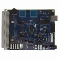
Manufacturer Part Number
C8051F930-TB
Description
BOARD TARGET/PROTO W/C8051F930
Manufacturer
Silicon Laboratories Inc
Type
MCUr
Specifications of C8051F930-TB
Contents
Board
Processor To Be Evaluated
C8051F930
Processor Series
C8051F9xx
Data Bus Width
8 bit
Interface Type
I2C, UART, SPI
Maximum Operating Temperature
+ 85 C
Minimum Operating Temperature
- 40 C
Operating Supply Voltage
0.9 V to 3.6 V
Lead Free Status / RoHS Status
Lead free / RoHS Compliant
For Use With/related Products
C8051F930
Lead Free Status / Rohs Status
Lead free / RoHS Compliant
Other names
336-1472


C8051F930-DK
7.6. Expansion I/O Connector (P1)
The 96-pin Expansion I/O connector P1 provides access to all signal pins of the C8051F930 device (except the C2
debug interface signals). In addition, power supply and ground pins are included. A small through-hole prototyping
area is also provided. See Table 2 for a list of pin descriptions for P1.
18
Row A
Pin #
10
11
12
13
14
15
16
17
18
19
20
21
22
23
24
25
26
27
28
29
30
31
32
1
2
3
4
5
6
7
8
9
Description
P1.7/AD7
P1.4/AD4
P1.1/AD1
P2.2/A10
P2.3/A11
A6-Latch
A3-Latch
A0-Latch
P0.5/RX
P2.0/A8
+3 VD
P0.2H
GND
/WR
nc
nc
nc
nc
nc
nc
nc
nc
nc
nc
nc
nc
nc
nc
nc
nc
nc
nc
Table 2. P1 Pin Descriptions
Row B
Pin #
10
11
12
13
14
15
16
17
18
19
20
21
22
23
24
25
26
27
28
29
30
31
32
1
2
3
4
5
6
7
8
9
Rev. 0.5
Description
P0.7/IREF0
P0.1/AGND
VDD/DC+
P1.6/AD6
P1.3/AD3
P1.0/AD0
A5-Latch
A2-Latch
P2.3/A11
P2.2/A10
P0.4/TX
P2.1/A9
GND
GND
GND
ALE
/RD
nc
nc
nc
nc
nc
nc
nc
nc
nc
nc
nc
nc
nc
nc
nc
Row C
Pin #
10
12
13
14
15
16
17
18
19
20
21
22
23
24
25
26
27
28
29
30
31
32
11
1
2
3
4
5
6
7
8
9
P0.6/CNVSTR
Description
P0.0/VREF
P1.5/AD5
P1.2/AD2
A7-Latch
A4-Latch
A1-Latch
P2.3/A11
P2.0/A8
P2.1/A9
P0.3H
P0.2H
VBAT
nc
nc
nc
nc
nc
nc
nc
nc
nc
nc
nc
nc
nc
nc
nc
nc
nc
nc
nc
Related parts for C8051F930-TB
Image
Part Number
Description
Manufacturer
Datasheet
Request
R

Part Number:
Description:
SMD/C°/SINGLE-ENDED OUTPUT SILICON OSCILLATOR
Manufacturer:
Silicon Laboratories Inc
Part Number:
Description:
Manufacturer:
Silicon Laboratories Inc
Datasheet:
Part Number:
Description:
N/A N/A/SI4010 AES KEYFOB DEMO WITH LCD RX
Manufacturer:
Silicon Laboratories Inc
Datasheet:
Part Number:
Description:
N/A N/A/SI4010 SIMPLIFIED KEY FOB DEMO WITH LED RX
Manufacturer:
Silicon Laboratories Inc
Datasheet:
Part Number:
Description:
N/A/-40 TO 85 OC/EZLINK MODULE; F930/4432 HIGH BAND (REV E/B1)
Manufacturer:
Silicon Laboratories Inc
Part Number:
Description:
EZLink Module; F930/4432 Low Band (rev e/B1)
Manufacturer:
Silicon Laboratories Inc
Part Number:
Description:
I°/4460 10 DBM RADIO TEST CARD 434 MHZ
Manufacturer:
Silicon Laboratories Inc
Part Number:
Description:
I°/4461 14 DBM RADIO TEST CARD 868 MHZ
Manufacturer:
Silicon Laboratories Inc
Part Number:
Description:
I°/4463 20 DBM RFSWITCH RADIO TEST CARD 460 MHZ
Manufacturer:
Silicon Laboratories Inc
Part Number:
Description:
I°/4463 20 DBM RADIO TEST CARD 868 MHZ
Manufacturer:
Silicon Laboratories Inc
Part Number:
Description:
I°/4463 27 DBM RADIO TEST CARD 868 MHZ
Manufacturer:
Silicon Laboratories Inc
Part Number:
Description:
I°/4463 SKYWORKS 30 DBM RADIO TEST CARD 915 MHZ
Manufacturer:
Silicon Laboratories Inc
Part Number:
Description:
N/A N/A/-40 TO 85 OC/4463 RFMD 30 DBM RADIO TEST CARD 915 MHZ
Manufacturer:
Silicon Laboratories Inc
Part Number:
Description:
I°/4463 20 DBM RADIO TEST CARD 169 MHZ
Manufacturer:
Silicon Laboratories Inc