MPC8349E-MITX-GP Freescale Semiconductor, MPC8349E-MITX-GP Datasheet - Page 21
MPC8349E-MITX-GP
Manufacturer Part Number
MPC8349E-MITX-GP
Description
KIT REFERENCE PLATFORM MPC8349E
Manufacturer
Freescale Semiconductor
Series
PowerQUICC II™ PROr
Type
MPUr
Datasheets
1.MPC8349E-MITX-GP.pdf
(36 pages)
2.MPC8349E-MITX-GP.pdf
(2 pages)
3.MPC8349E-MITX-GP.pdf
(1 pages)
Specifications of MPC8349E-MITX-GP
Contents
Module and Misc Hardware
For Use With/related Products
MPC8349E
Lead Free Status / RoHS Status
Lead free / RoHS Compliant


1.6.3
An M66EN input pin determines the AC timing of the PCI interface. On the MPC8349E-mITX-GP board,
the state of this signal can be driven to 0 by the J22 jumper to select 33 MHz AC timing. If J22.F is not
driven to 0, the M66EN signal level is determined by the PCI agent card connected to PCI slot P1. If a 33
MHz only card is inserted, the M66EN signal is driven to 0 by the PCI agent card according to the PCI
specification, or it is driven to 1 if it can perform at 66 MHz. See
1.6.4
The reset configuration word (RCW) controls the clock ratios and other basic device functions such as PCI
host or agent mode, boot location, TSEC modes, and endian mode. The reset configuration word is divided
into reset configuration word lower (RCWL) and reset configuration word higher (RCWH) and is loaded
from the local bus during the power-on or hard reset flow. The default RCW low bit setting is
0x0404_0000. The default RCW high bit setting is 0xB460_A000.
The RCW is located at the lowest 64 bytes of the boot Flash memory, which is 0xFE00_0000 if the default
memory map is used.
Freescale Semiconductor
.
Jumper Off
Jumper On
J22.F
PCI Operating Frequency
Reset Configuration Word
M66EN signal is determined by the card plugged into the PCI slot.
M66EN signal is hardwired to 0, which is hard coded to 33 MHz PCI operation.
Jumper Off
Jumper On
MPC8349E-mITX-GP Reference Design Platform User’s Guide, Rev. 0
J22.G
FE000000:
FE000010:
FE000020:
FE000030:
Table 12. M66EN Signal Status Selection
Serial EEPROM is write protected (WC not asserted).
Serial EEPROM is not write protected (WC asserted).
Table 13. Default RCW in Flash Memory
Preliminary—Subject to Change Without Notice
B0B0B0B0
A0A0A0A0
04040404
00000000
Table 11. EEPROM Write Protect
B0B0B0B0
A0A0A0A0
Address
04040404
00000000
Description
Description
04040404
00000000
60606060
00000000
Table
12.
04040404
00000000
60606060
00000000
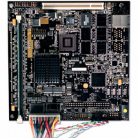
MPC8349E-mITX-GP Board
21
Related parts for MPC8349E-MITX-GP
Image
Part Number
Description
Manufacturer
Datasheet
Request
R

Part Number:
Description:
BOARD REFERENCE FOR MPC8349
Manufacturer:
Freescale Semiconductor
Datasheet:

Part Number:
Description:
KIT MODULAR DEV SYSTEM MPC8349E
Manufacturer:
Freescale Semiconductor
Datasheet:

Part Number:
Description:
MCU, MPU & DSP Development Tools PROCESSR BD MPC8349E
Manufacturer:
Freescale Semiconductor
Part Number:
Description:
MCU, MPU & DSP Development Tools KIT FOR MPC8349E BDS
Manufacturer:
Freescale Semiconductor

Part Number:
Description:
Manufacturer:
Freescale Semiconductor, Inc
Datasheet:
Part Number:
Description:
Manufacturer:
Freescale Semiconductor, Inc
Datasheet:
Part Number:
Description:
Manufacturer:
Freescale Semiconductor, Inc
Datasheet:
Part Number:
Description:
Manufacturer:
Freescale Semiconductor, Inc
Datasheet:
Part Number:
Description:
Manufacturer:
Freescale Semiconductor, Inc
Datasheet:
Part Number:
Description:
Manufacturer:
Freescale Semiconductor, Inc
Datasheet:
Part Number:
Description:
Manufacturer:
Freescale Semiconductor, Inc
Datasheet:
Part Number:
Description:
Manufacturer:
Freescale Semiconductor, Inc
Datasheet:
Part Number:
Description:
Manufacturer:
Freescale Semiconductor, Inc
Datasheet:
Part Number:
Description:
Manufacturer:
Freescale Semiconductor, Inc
Datasheet:
Part Number:
Description:
Manufacturer:
Freescale Semiconductor, Inc
Datasheet: