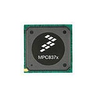
MPC8377E-RDBA Freescale Semiconductor, MPC8377E-RDBA Datasheet - Page 51

MPC8377E-RDBA
Manufacturer Part Number
MPC8377E-RDBA
Description
BOARD REF DES MPC8377 REV 2.1
Manufacturer
Freescale Semiconductor
Series
PowerQUICC II™ PROr
Type
MPUr
Datasheets
1.MPC8377EVRAGD.pdf
(126 pages)
2.MPC8377EVRAGD.pdf
(2 pages)
3.MPC8377E-RDBA.pdf
(2 pages)
Specifications of MPC8377E-RDBA
Design Resources
MPC8379E-RDB Ref Design Guide
Contents
Board, CD
Frequency
667 MHz
For Use With/related Products
MPC8377E
Lead Free Status / RoHS Status
Lead free / RoHS Compliant
- Current page: 51 of 126
- Download datasheet (3Mb)
11.3.1.2
The following equations show how to calculate the allowed skew range between the SD_CLK and
SD_DAT/CMD signals on the PCB.
This means that clock can be delayed versus data up to 8 ns (external delay line) in ideal case of
t
11.3.2
Figure 31
For the input path, the device eSDHC expects to sample the data 1.5 internal clock cycles after it was
driven by the SD card. Since in this mode the SD card drives the data at the rising edge of the clock, a
sufficient delay to the clock and the data must exist to ensure it will not be sampled at the wrong internal
clock falling edge. Note that the internal clock which is guaranteed to be 50% duty cycle is used to sample
the data, and therefore used in the equations.
Freescale Semiconductor
SHSCLKL
t
t
MPC8377E Pins
CLK_DELAY
CLK_DELAY
Output from the
MPC8377E Pin
SD CLK at the
SD Card Pins
= 10 ns:
provides the data and command input timing diagram.
the Card Pin
High-Speed Input Path (Read)
Input at the
SD CLK at
High-Speed Write Meeting Hold (Minimum Delay)
MPC8377E PowerQUICC II Pro Processor Hardware Specifications, Rev. 4
–
–
t
t
DATA_DELAY
DATA_DELAY
t
t
CLK_DELAY
CLK_DELAY
Driving
Edge
t
1/2 Cycle
ODLY
t
OH
t
< t
–
SHSCK
< 10 + 0
< 8
Figure 31. High-Speed Input Path
t
DATA_DELAY
SHSCKL
t
CLK_DELAY
(Clock Cycle)
+ t
–
Wrong Edge
2
(MPC8377E Input Setup)
SHSKHOX
< t
SHSCKL
t
DATA_DELAY
+ t
+ t
DATA_DELAY
t
SHSKHOX
SHSIVKH
Enhanced Secure Digital Host Controller (eSDHC)
–
–
t
t
IH
IH
Right Edge
Sampling
Edge
(MPC8377E Input Hold)
t
SHSIXKH
Eqn. 13
Eqn. 14
51
Related parts for MPC8377E-RDBA
Image
Part Number
Description
Manufacturer
Datasheet
Request
R
Part Number:
Description:
BOARD MODULAR DEV SYSTEM
Manufacturer:
Freescale Semiconductor
Datasheet:
Part Number:
Description:
PowerQUICC II Pro Processor
Manufacturer:
Freescale Semiconductor
Part Number:
Description:
Manufacturer:
Freescale Semiconductor, Inc
Datasheet:
Part Number:
Description:
Manufacturer:
Freescale Semiconductor, Inc
Datasheet:
Part Number:
Description:
Manufacturer:
Freescale Semiconductor, Inc
Datasheet:
Part Number:
Description:
Manufacturer:
Freescale Semiconductor, Inc
Datasheet:
Part Number:
Description:
Manufacturer:
Freescale Semiconductor, Inc
Datasheet:
Part Number:
Description:
Manufacturer:
Freescale Semiconductor, Inc
Datasheet:
Part Number:
Description:
Manufacturer:
Freescale Semiconductor, Inc
Datasheet:
Part Number:
Description:
Manufacturer:
Freescale Semiconductor, Inc
Datasheet:
Part Number:
Description:
Manufacturer:
Freescale Semiconductor, Inc
Datasheet:
Part Number:
Description:
Manufacturer:
Freescale Semiconductor, Inc
Datasheet:
Part Number:
Description:
Manufacturer:
Freescale Semiconductor, Inc
Datasheet:
Part Number:
Description:
Manufacturer:
Freescale Semiconductor, Inc
Datasheet:
Part Number:
Description:
Manufacturer:
Freescale Semiconductor, Inc
Datasheet:


