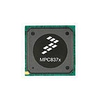
MPC8377E-RDBA Freescale Semiconductor, MPC8377E-RDBA Datasheet - Page 64

MPC8377E-RDBA
Manufacturer Part Number
MPC8377E-RDBA
Description
BOARD REF DES MPC8377 REV 2.1
Manufacturer
Freescale Semiconductor
Series
PowerQUICC II™ PROr
Type
MPUr
Datasheets
1.MPC8377EVRAGD.pdf
(126 pages)
2.MPC8377EVRAGD.pdf
(2 pages)
3.MPC8377E-RDBA.pdf
(2 pages)
Specifications of MPC8377E-RDBA
Design Resources
MPC8379E-RDB Ref Design Guide
Contents
Board, CD
Frequency
667 MHz
For Use With/related Products
MPC8377E
Lead Free Status / RoHS Status
Lead free / RoHS Compliant
PCI Express
15.4.2
The Tx eye diagram in
Figure
must be met for the transmitter. Both diagrams must be aligned in time using the jitter median to locate the
center of the eye diagram. The different eye diagrams differ in voltage depending on whether it is a
64
Common mode return
loss
DC differential Tx
impedance
Transmitter DC
impedance
Lane-to-Lane output
skew
AC coupling capacitor
Crosslink random
timeout
Note:
1
2
3
4
5
6
7
No test load is necessarily associated with this value.
Specified at the measurement point into a timing and voltage compliance test load as shown in
any 250 consecutive Tx UIs. (Also refer to the transmitter compliance eye diagram shown in
A T
transmitter collected over any 250 consecutive Tx UIs. The T
Tx jitter budget collected over any 250 consecutive Tx UIs. It should be noted that the median is not the same as the mean.
The jitter median describes the point in time where the number of jitter points on either side is approximately equal as opposed
to the averaged time value.
The transmitter input impedance will result in a differential return loss greater than or equal to 12 dB and a common mode
return loss greater than or equal to 6 dB over a frequency range of 50 MHz to 1.25 GHz. This input impedance requirement
applies to all valid input levels. The reference impedance for return loss measurements is 50 Ω to ground for both the D+ and
D– line (that is, as measured by a vector network analyzer with 50-Ω probes, see
C
Measured between 20%–80% at transmitter package pins into a test load as shown in
See Section 4.3.1.8 of the PCI Express Base Specifications, Rev 1.0a.
See Section 4.2.6.3 of the PCI Express Base Specifications, Rev 1.0a.
TX
TX-EYE
Parameter
, is optional for the return loss measurement.
44) in place of any real PCI Express interconnect + Rx component. There are two eye diagrams that
= 0.70 UI provides for a total sum of deterministic and random jitter budget of T
Transmitter Compliance Eye Diagrams
Table 52. Differential Transmitter (Tx) Output Specifications (continued)
MPC8377E PowerQUICC II Pro Processor Hardware Specifications, Rev. 4
Measured over 50 MHz to
1.25 GHz.
Tx DC differential mode low
impedance
Required Tx D+ as well as D–
DC impedance during all
states
Static skew between any two
transmitter lanes within a
single link
All transmitters should be AC
coupled. The AC coupling is
required either within the
media or within the
transmitting component itself.
This random timeout helps
resolve conflicts in crosslink
configuration by eventually
resulting in only one
downstream and one
upstream port.
Figure 42
Conditions
is specified using the passive compliance/test measurement load (see
Z
L
TX-DIFF-DC
RL
T
Symbol
Z
TX-SKEW
TX-EYE-MEDIAN-to-MAX-JITTER
crosslink
TX-DC
C
TX-CM
TX
Min
80
40
75
—
6
0
Figure
Figure 44
Typical
44). Note that the series capacitors,
median is less than half of the total
100
—
—
—
—
—
TX-JITTER-MAX
Figure
Figure 44
for both V
Freescale Semiconductor
500 +
42.)
Max
2 UI
120
200
—
—
1
and measured over
= 0.30 UI for the
TX-D+
Units
ms
dB
nF
ps
Ω
Ω
and V
Notes
TX-D-
—
—
—
—
4
7
.


