HW-V5-ML555-G Xilinx Inc, HW-V5-ML555-G Datasheet - Page 62
HW-V5-ML555-G
Manufacturer Part Number
HW-V5-ML555-G
Description
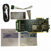
BOARD EVAL FOR VIRTEX-5 ML555
Manufacturer
Xilinx Inc
Series
Virtex™ -5r
Type
FPGAr
Datasheet
1.HW-V5-PCIE2-UNI-G.pdf
(108 pages)
Specifications of HW-V5-ML555-G
Contents
Board, Cables, CD
Silicon Manufacturer
Xilinx
Features
Parallel Connectivity, Three On-board Clock Sources
Kit Contents
Board, Cables, CD, Power Supply
Silicon Family Name
Virtex-5
Silicon Core Number
XC5VLX50T-1FF1136
Rohs Compliant
Yes
Lead Free Status / RoHS Status
Lead free / RoHS Compliant
For Use With/related Products
Virtex™-5 FPGA
For Use With
HW-AFX-SMA-SFP - CONVERSION MODULE SMA - SFPHW-AFX-SMA-SATA - CONVERSION MODULE SMA - SATAHW-AFX-SMA-RJ45 - CONVERSION MODULE SMA - RJ45HW-AFX-SMA-HSSDC2 - CONVERSION MODULE SMA - HSSDC2HW-AFX-BERG-EPHY - DAUGHTER CARD PHY BERG-EPHY
Lead Free Status / RoHS Status
Lead free / RoHS Compliant, Lead free / RoHS Compliant
Other names
122-1586
HW-V5-ML555-G
HW-V5-ML555-G
Available stocks
Company
Part Number
Manufacturer
Quantity
Price


Chapter 3: Hardware Description
62
Parallel Mode Operation
Table 3-21: ICS8442 Divisor Switch Settings
Each clock synthesizer has one set of subminiature DIP switches to set the multiplier and
divider settings in parallel mode. Clock Synthesizer 1, with a 10 MHz reference clock
input, can be set to 0x019 through 0x046, as shown in
Synthesizer 2, with a 25 MHz reference clock input, can be set to 0x00A through 0x01C, as
shown in
selection of multiplier values that result in valid VCO lock ranges. Multiplier bits that
would result in a VCO unlock condition are hardwired to a logic 0 level on the board.
Notes:
1. A logic “0” is obtained by moving the switch to the “OPEN” position, and a logic “1” is obtained by
2. SW12-9 is for the N1 input of Clock Synthesizer 1, and SW12-10 is for the N1 input of Clock
3. SW10-9 is for the N0 input of Clock Synthesizer 1, and SW12-11 is for the N0 input of Clock Synthesizer
Figure 3-11
moving the switch to the “CLOSED” position.
Synthesizer 2.
2.
SW12-10
SW12-9 or
“N1”
0
0
1
1
Table 3-23, page
shows the locations of the switches for both synthesizers.
(2)
SW12-11
SW10-9 or
www.xilinx.com
“N0”
66. DIP switches are provided on the board to allow user
0
1
0
1
(3)
Output Divisor
Value
1
2
4
8
Virtex-5 FPGA ML555 Development Kit
Table 3-22, page
Minimum
Output Frequency (MHz)
31.25
62.5
250
125
UG201 (v1.4) March 10, 2008
64. Clock
Maximum
87.5
700
350
175
R
Related parts for HW-V5-ML555-G
Image
Part Number
Description
Manufacturer
Datasheet
Request
R

Part Number:
Description:
EVAL PLATFORM V5 FXT
Manufacturer:
Xilinx Inc
Datasheet:

Part Number:
Description:
BOARD EVAL FOR VIRTEX-5
Manufacturer:
Xilinx Inc
Datasheet:
Part Number:
Description:
BOARD EVAL FOR VIRTEX-5
Manufacturer:
Xilinx Inc
Datasheet:

Part Number:
Description:
EVALUATION PLATFORM VIRTEX-5
Manufacturer:
Xilinx Inc
Datasheet:

Part Number:
Description:
EVALUATION PLATFORM VIRTEX-5
Manufacturer:
Xilinx Inc
Datasheet:
Part Number:
Description:
KIT DEV PCIEXPRESS GTX VIRTEX5
Manufacturer:
Xilinx Inc
Datasheet:

Part Number:
Description:
EVALUATION PLATFORM VIRTEX-5
Manufacturer:
Xilinx Inc
Datasheet:
Part Number:
Description:
BOARD EVAL FOR VIRTEX-5 ML510
Manufacturer:
Xilinx Inc
Datasheet:
Part Number:
Description:
EVALUATION PLATFORM VIRTEX-5
Manufacturer:
Xilinx Inc
Datasheet:
Part Number:
Description:
CoolRunner-II CPLD
Manufacturer:
XILINX [Xilinx, Inc]
Datasheet:
Part Number:
Description:
In-System Programmable CPLD
Manufacturer:
XILINX [Xilinx, Inc]
Datasheet:
Part Number:
Description:
High-Performance CPLD
Manufacturer:
XILINX [Xilinx, Inc]
Datasheet:
Part Number:
Description:
XCR3128XL 128 Macrocell CPLD
Manufacturer:
XILINX [Xilinx, Inc]
Datasheet:
Part Number:
Description:
XC95288XL High Performance CPLD
Manufacturer:
XILINX [Xilinx, Inc]
Datasheet: