AD8362-EVAL Analog Devices Inc, AD8362-EVAL Datasheet - Page 26
AD8362-EVAL
Manufacturer Part Number
AD8362-EVAL
Description
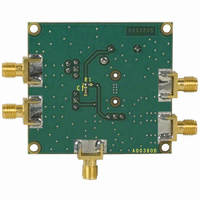
BOARD EVAL FOR AD8362
Manufacturer
Analog Devices Inc
Datasheet
1.AD8362-EVAL.pdf
(32 pages)
Specifications of AD8362-EVAL
Rohs Status
RoHS non-compliant


AD8362
OPERATION IN CONTROLLER MODE
The AD8362 provides a controller mode feature at the VOUT
pin. Using VSET for the setpoint voltage, it is possible for the
AD8362 to control subsystems such as power amplifiers (PAs),
VGAs, or variable voltage attenuators (VVAs), which have
output power that decreases monotonically with respect to
their (increasing) gain control signal.
P
OUT
ATTN
1000pF
C10
Figure 64. Basic Connections for Controller Mode Operation
1:4 Z-RATIO
ETC1.6-4-2-3
T1
100pF
100pF
C6
C5
1000pF
OUTPUT CONTROL VOLTAGE
1nF
C4
C8
1nF
C7
1
2
3
4
5
6
7
8
COMM
CHPF
DECL
INHI
INLO
DECL
PWDN
COMM
0.1V TO 4.9V
AD8362
OUTPUT
CONTROLLED SYSTEM
VAPC INCREASES)
(OUTPUT POWER
DECREASES AS
ACOM
ACOM
VPOS
VOUT
VREF
VTGT
VSET
CLPF
VAPC
(SEE TEXT)
16
15
14
13
12
11
10
9
C3
INPUT
SETPOINT
VOLTAGE
INPUT
0V TO 3.5V
V
S
0.1µF
1nF
C1
C2
P
Rev. D | Page 26 of 32
IN
To operate in controller mode, the link between VSET and
VOUT is broken. A setpoint voltage is applied to the VSET
input, while VOUT is connected to the gain control terminal
of the VGA, and the AD8362 RF input is connected to the out-
put of the VGA (generally using a directional coupler or power
splitter and some additional attenuation). Based on the defined
relationship between VOUT and the RF input signal when the
device is in measurement mode, the AD8362 adjusts the voltage
on VOUT (VOUT is now an error amplifier output) until the
level at the RF input corresponds to the applied VSET. For
example, in a closed loop system, if VSET is set to 3 V, VOUT
increases or decreases until the input signal is equal to 0 dBm.
This relationship follows directly from the measurement mode
transfer function (see Figure 10, Figure 11, and Figure 12).
Therefore, when the AD8362 operates in controller mode, there
is no defined relationship between VSET and VOUT. VOUT
settles to a value that results in balance between the input signal
levels appearing at INHI/INLO and VSET.
For this output power control loop to be stable, a ground-
referenced capacitor must be connected to the CLPF pin.
This capacitor integrates the internal error current that is
present when the loop is not balanced.
Increasing VSET, which corresponds to demanding a higher
signal from the VGA, tends to decrease VOUT. The VGA or VVA
therefore must have a negative sense. In other words, increasing
the gain control voltage decreases gain. If this is not the case, an
op amp, configured as an inverter with suitable level shifting, can
be used to correct the sense of the VOUT signal.
Related parts for AD8362-EVAL
Image
Part Number
Description
Manufacturer
Datasheet
Request
R

Part Number:
Description:
BOARD EVAL FOR AD8362
Manufacturer:
Analog Devices Inc
Datasheet:

Part Number:
Description:
±1.7g Dual-Axis IMEMS Accelerometer Evaluation Board
Manufacturer:
Analog Devices Inc
Datasheet:
Part Number:
Description:
Inertial Sensor Evaluation System
Manufacturer:
Analog Devices Inc
Datasheet:
Part Number:
Description:
Manufacturer:
Analog Devices Inc
Datasheet:
Part Number:
Description:
Manufacturer:
Analog Devices Inc
Datasheet:
Part Number:
Description:
Manufacturer:
Analog Devices Inc
Datasheet:
Part Number:
Description:
Manufacturer:
Analog Devices Inc
Datasheet:
Part Number:
Description:
Manufacturer:
Analog Devices Inc
Datasheet:
Part Number:
Description:
Manufacturer:
Analog Devices Inc
Datasheet:
Part Number:
Description:
Manufacturer:
Analog Devices Inc
Datasheet:
Part Number:
Description:
Manufacturer:
Analog Devices Inc
Datasheet:
Part Number:
Description:
Manufacturer:
Analog Devices Inc
Datasheet:
Part Number:
Description:
Manufacturer:
Analog Devices Inc
Datasheet: