EVAL-ADUC7024QS Analog Devices Inc, EVAL-ADUC7024QS Datasheet - Page 2
EVAL-ADUC7024QS
Manufacturer Part Number
EVAL-ADUC7024QS
Description
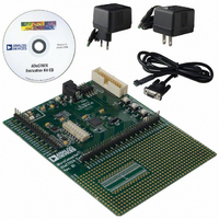
KIT DEV FOR ADUC7024/7025
Manufacturer
Analog Devices Inc
Series
QuickStart™ Kitr
Type
ARM7 Processor, Microcontrollerr
Datasheet
1.EVAL-ADUC7024QS.pdf
(4 pages)
Specifications of EVAL-ADUC7024QS
Mfg Application Notes
ADUC7024 Eval Board/Dev System, AN-719
Contents
Evaluation Board, Power Supply, Cable, Software and Documentation
For Use With/related Products
ADuC7024
Lead Free Status / RoHS Status
Contains lead / RoHS non-compliant
Other names
EVAL-ADUC7024QS-U2


ADuC7019/ADuC702x
ANOMALIES
ADuC7019/ADuC702x Functionality Issues
1. ADC Conversion Start Mode [er017]:
Background:
Issue:
Workaround:
Related Issues:
2. MMR Default Values [er018]:
Background:
Issue:
Workaround:
Related Issues:
3. On-Chip Loader’s Protection Command [er019]:
Background:
Issue:
Workaround:
Related Issues:
ADCCON [2:0] allow the user to select one of six ADC conversion start modes of operation, namely:
• External pin (P2.0) triggered ADC conversion
• Timer1 overflow
• Timer0 overflow
• Single software conversion
• Continuous software conversion
•
The active-low, external pin (P2.0) triggered conversion is always active, even if it is not selected via ADCCON [2:0].
This is the case if the function of P2.0 is configured as a CONV
for example, SOUT, PLAO[5], or GPIO. This means that if a falling edge is seen on P2.0, a single ADC conversion is
triggered if ADCCON [7] is enabled. If an ADC conversion cycle is already in progress, this conversion stops and a new
ADC conversion cycle begins in response to a falling edge on P2.0.
Pending.
ADCCON [7], the ADC enable conversion mode bit, is fully functional, allowing the user to disable any of the active
ADC conversion modes except continuous conversion (see the
data
The on-chip factory firmware allows downloading to the ADuC7019/ADuC702x parts through the UART or I
interfaces. After kernel execution, in normal mode or after downloading and jumping to user code, the MMR default
values should be as described in the datasheet (see the
When downloading occurs via one of these interfaces and a software RUN command is sent (as described in
AN-806), the following MMRs are modified by the factory firmware:
UART loader (standard parts)
COMTX
COMRX
COMDIV0
COMCON0
COMDIV2
GP1CON
FEEADR
GP1CON needs to be configured to use P1.0 and P1.1 as GPIO.
COMDIV2 must be cleared to use the UART without the fractional divider on standard parts.
No MMRs are modified as a result of running user code from a power cycle, toggling of the reset pin, or a software reset.
The on-chip factory firmware residing in 2 kB of Flash/EE memory allows the downloading of user code to user space in
Flash/EE via a serial port (either UART or I
protection of the Flash/EE user space through the use of a 32-bit key.
The protection key is a 32-bit value that should be entered in FEEADR and FEEDAT during the protection sequence.
The loader ignores the 16 MSB of the key and writes only the 16 LSB in both FEEADR and FEEDAT.
None.
This does not affect writing keys via JTAG or user code.
PLA triggered ADC conversion
sheet).
2
C, depending on the model). After downloading code, it also allows
Rev. B | Page 2 of 4
ADuC7019/7020/7021/7022/7024/7025/7026/7027 data
I
I2C0SRX
I2C0STX
I2C0CFG
I2C0ID0/1/2/3
I2C0STA
GP1CON
FEEADR
START
2
C loader (I models)
ADuC7019/7020/7021/7022/7024/7025/7026/7027
input or if P2.0 is configured as any other function,
2
C®
AN-724
sheet).
or
Related parts for EVAL-ADUC7024QS
Image
Part Number
Description
Manufacturer
Datasheet
Request
R


Part Number:
Description:
BOARD EVAL FOR SI270X-A
Manufacturer:
Silicon Laboratories Inc
Datasheet:

Part Number:
Description:
BUCK CONV REF DESIGN KIT IP1201
Manufacturer:
International Rectifier
Datasheet:
Part Number:
Description:
BOARD DEMO SYNC DUAL BUCK CNVTER
Manufacturer:
International Rectifier
Datasheet:
Part Number:
Description:
BOARD DEMO SYNC BUCK CONVETER
Manufacturer:
International Rectifier
Datasheet:

Part Number:
Description:
EVALBOARD/EB Omnidirectional microphone - Analog
Manufacturer:
Analog Devices
Datasheet:
Part Number:
Description:
EVALBOARD/EB Omnidirectional microphone - Analog
Manufacturer:
Analog Devices
Datasheet:


Part Number:
Description:
BOARD EVAL LED DRIVER LT3756
Manufacturer:
Linear Technology
Datasheet:

Part Number:
Description:
BOARD EVAL FOR AD7741/7742
Manufacturer:
Analog Devices Inc
Datasheet:

Part Number:
Description:
±1.7g Dual-Axis IMEMS Accelerometer Evaluation Board
Manufacturer:
Analog Devices Inc
Datasheet:

Part Number:
Description:
IC MULTIPLIER ANALOG 8-SOIC T/R
Manufacturer:
Analog Devices Inc
Datasheet:

Part Number:
Description:
IC ANALOG MULTIPLIER 8-DIP
Manufacturer:
Analog Devices Inc
Datasheet:
Part Number:
Description:
IC ANALOG MULTIPLIER 8-SOIC
Manufacturer:
Analog Devices Inc
Datasheet:
Part Number:
Description:
IC ANALOG MULTIPLIER 8-DIP
Manufacturer:
Analog Devices Inc
Datasheet: