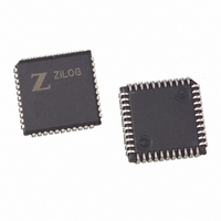
Z86E4000ZDV Zilog, Z86E4000ZDV Datasheet - Page 24

Z86E4000ZDV
Manufacturer Part Number
Z86E4000ZDV
Description
44 PIN PLCC ADAPTER
Manufacturer
Zilog
Datasheet
1.Z86E4001ZDV.pdf
(64 pages)
Specifications of Z86E4000ZDV
Convert From (adapter End)
40-Pin DIP ZIF Socket
Convert To (adapter End)
44-PLCC Plug
For Use With/related Products
Zilog Emulators/Programmers
Lead Free Status / RoHS Status
Contains lead / RoHS non-compliant
Other names
269-2015
Z86E30/E31/E40
Z8 4K OTP Microcontroller
PIN FUNCTIONS
EPROM Programming Mode
D7–D0 Data Bus. The data can be read from or written to
external memory through the data bus.
A11–A0 Address Bus. During programming, the EPROM
address is written to the address bus.
V
EPROM read mode and 6V during other modes.
CE Chip Enable (active Low). This pin is active during
EPROM Read Mode, Program Mode, and Program Verify
Mode.
OE Output Enable (active Low). This pin drives the direc-
tion of the Data Bus. When this pin is Low, the Data Bus is
output, when High, the Data Bus is input.
EPM EPROM Program Mode. This pin controls the differ-
ent EPROM Program Mode by applying different voltages.
V
age.
PGM Program Mode (active Low). When this pin is Low,
the data is programmed to the EPROM through the Data
Bus.
Application Precaution
The production test-mode environment may be enabled
accidentally during normal operation if excessive noise
surges above V
In addition, processor operation of Z8 OTP devices may be
affected by excessive noise surges on the V
OE pins while the microcontroller is in Standard Mode.
Recommendations for dampening voltage surges in both
test and OTP mode include the following:
Standard Mode
XTAL Crystal 1 (time-based input). This pin connects a
parallel-resonant crystal, ceramic resonator, LC, RC net-
work, or external single-phase clock to the on-chip oscilla-
tor input.
XTAL2 Crystal 2 (time-based output). This pin connects a
parallel-resonant crystal, ceramic resonator, LC, or RC
network to the on-chip oscillator output.
24
CC
PP
Using a clamping diode to V
Adding a capacitor to the affected pin
Program Voltage. This pin supplies the program volt-
Power Supply. This pin must supply 5V during the
CC
occur on pins XTAL1 and RESET.
CC
PP
, CE, EPM,
P R E L I M I N A R Y
R/W Read/Write (output, write Low). The R/W signal is
Low when the CCP is writing to the external program or
data memory (Z86E40 only).
RESET Reset (input, active Low). Reset will initialize the
MCU. Reset is accomplished either through Power-On,
Watch-Dog Timer reset, STOP-Mode Recovery, or exter-
nal reset. During Power-On Reset and Watch-Dog Timer
Reset, the internally generated reset drives the reset pin
low for the POR time. Any devices driving the reset line
must be open-drain in order to avoid damage from a pos-
sible conflict during reset conditions. Pull-up is provided in-
ternally. After the POR time, RESET is a Schmitt-triggered
input.
To avoid asynchronous and noisy reset problems, the
Z86E40 is equipped with a reset filter of four external
clocks (4TpC). If the external reset signal is less than 4TpC
in duration, no reset occurs. On the fifth clock after the re-
set is detected, an internal RST signal is latched and held
for an internal register count of 18 external clocks, or for
the duration of the external reset, whichever is longer. Dur-
ing the reset cycle, DS is held active Low while AS cycles
at a rate of TpC/2. Program execution begins at location
000CH, 5–10 TpC cycles after RESET is released. For
Power-On Reset, the reset output time is 5 ms. The
Z86E40 does not reset WDTMR, SMR, P2M, and P3M
registers on a STOP-Mode Recovery operation.
ROMless (input, active Low). This pin, when connected to
GND, disables the internal ROM and forces the device to
function as a Z86C90/C89 ROMless Z8. (Note that, when
left unconnected or pulled High to V
tions normally as a Z8 ROM version).
Note: When using in ROM Mode in High EMI (noisy) envi-
ronment, the ROMless pins should be connected directly
to V
CC
.
CC
, the device func-
DS97Z8X0502
Zilog


