MPC566EVB Freescale Semiconductor, MPC566EVB Datasheet - Page 10
MPC566EVB
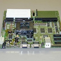
Manufacturer Part Number
MPC566EVB
Description
KIT EVALUATION FOR MPC565/566
Manufacturer
Freescale Semiconductor
Specifications of MPC566EVB
Processor To Be Evaluated
MPC56x
Data Bus Width
32 bit
Interface Type
RS-232, Ethernet
Lead Free Status / RoHS Status
Contains lead / RoHS non-compliant


Additional MPC565 Differences
3
The SRAM has three keep-alive power pins (VDDSRAM1, VDDSRAM2, and VDDSRAM3). These pins
provide keep-alive power to the SRAM arrays in the CALRAM modules and the DPTRAM modules.
The VDDSRAM1 pin powers the 32-Kbyte CALRAM A during keep-alive while power is off to the
MPC565 (except for the keep-alive power supplies). CALRAM A keeps all of its 32 Kbytes powered during
power down.
The VDDSRAM2 pin powers the 4-Kbyte CALRAM B module. The VDDSRAM3 pin powers the
DPTRAM modules during keep-alive as well as during normal operation. The CALRAM modules only
power their arrays from the VDDSRAM pins during keep-alive. During normal operation, they are powered
by the normal internal VDD of the part.
The DPTRAM modules (6 Kbytes and 4 Kbytes) and the 4-Kbyte DECRAM in the BBC module power their
arrays via the VDDSRAM3 pin during keep-alive and are supplied by VDD during normal operation.
4
The internal memory map is organized as a single 4-Mbyte block. This is shown in Figure 3. This block can
be moved to one of eight different locations. The internal memory space is divided into the following
sections:
The internal memory block can reside in one of eight possible 4-Mbyte memory spaces. These eight
locations are the first eight 4-Mbyte memory blocks starting with address 0x0000 0000, as shown in
Figure 2. There is a user programmable register in the USIU to configure the internal memory map to one
of the eight possible locations. Programmability of internal memory map location allows multiple chip
system.
The IMB3 address space block in Figure 3 shows memory allocation for IMB3 modules. It does not show
the actual memory space required for individual modules. All modules are mapped to the low address,
numerically, of the memory allocated for that module in the IMB3 address space.
10
•
•
•
•
•
•
CALRAM causes DSI exception only if the data relocation (DR) bit in the core machine state
register, MSR[DR], is set.
— L2U on MPC555 already followed this protocol, but the LRAM did not. Now all L-bus
— The MSR[DR] bit is described in the reference manual for more information.
Four additional PRDS control bits were added to the USIU to allow more granularity of PRDS
control on a part
BBC includes a 4-Kbyte DECRAM that can be used if compression is not used or is not available.
Flash memory (1 Mbyte) — U-bus memory
Static RAM memory (36 Kbytes CALRAM) — L-bus memory
Control registers and IMB3 modules (64 Kbytes), partitioned as
— USIU and flash control registers
— UIMB interface and IMB3 modules
— CALRAM and READI control registers (L-bus control register space)
SRAM Keep-Alive Power Behavior
MPC565 Memory Map
peripherals follow this protocol.
Freescale Semiconductor, Inc.
For More Information On This Product,
MPC565/MPC566 Product Brief
Go to: www.freescale.com
MOTOROLA
Related parts for MPC566EVB
Image
Part Number
Description
Manufacturer
Datasheet
Request
R

Part Number:
Description:
Manufacturer:
Freescale Semiconductor, Inc
Datasheet:
Part Number:
Description:
Manufacturer:
Freescale Semiconductor, Inc
Datasheet:
Part Number:
Description:
Manufacturer:
Freescale Semiconductor, Inc
Datasheet:
Part Number:
Description:
Manufacturer:
Freescale Semiconductor, Inc
Datasheet:
Part Number:
Description:
Manufacturer:
Freescale Semiconductor, Inc
Datasheet:
Part Number:
Description:
Manufacturer:
Freescale Semiconductor, Inc
Datasheet:
Part Number:
Description:
Manufacturer:
Freescale Semiconductor, Inc
Datasheet:
Part Number:
Description:
Manufacturer:
Freescale Semiconductor, Inc
Datasheet:
Part Number:
Description:
Manufacturer:
Freescale Semiconductor, Inc
Datasheet:
Part Number:
Description:
Manufacturer:
Freescale Semiconductor, Inc
Datasheet:
Part Number:
Description:
Manufacturer:
Freescale Semiconductor, Inc
Datasheet:
Part Number:
Description:
Manufacturer:
Freescale Semiconductor, Inc
Datasheet:
Part Number:
Description:
Manufacturer:
Freescale Semiconductor, Inc
Datasheet:
Part Number:
Description:
Manufacturer:
Freescale Semiconductor, Inc
Datasheet:
Part Number:
Description:
Manufacturer:
Freescale Semiconductor, Inc
Datasheet: