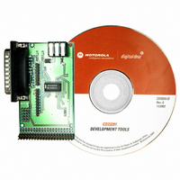
KIT33291DWEVB Freescale Semiconductor, KIT33291DWEVB Datasheet - Page 12

KIT33291DWEVB
Manufacturer Part Number
KIT33291DWEVB
Description
KIT EVAL FOR MC33291 SMART SW
Manufacturer
Freescale Semiconductor
Datasheet
1.MCZ33291EGR2.pdf
(27 pages)
Specifications of KIT33291DWEVB
Main Purpose
Power Management, Low Side Driver (Internal FET)
Embedded
No
Utilized Ic / Part
MC33291
Primary Attributes
8 Channel Internal Switch
Secondary Attributes
Overvoltage, Short-Circuit & Thermal Protection
Lead Free Status / RoHS Status
Contains lead / RoHS non-compliant
developed for automotive applications. It is an eight-output
low-side power switch having 8-bit serial control. The 33291
incorporates SMARTMOS technology having CMOS logic,
bipolar/MOS analog circuitry, and independent state of the
art double diffused MOS (DMOS) power output transistors.
Many benefits are realized as a direct result of using this
mixed technology. A simplified block diagram delineates
33291 in
current for their operation, structured MOS devices, since
they are voltage controlled, require only transient gate
charging current affording a significant decrease in power
consumption. The CMOS capability of the SMARTMOS
process allows significant amounts of logic to be
economically incorporated into the monolithic design.
Additionally, the bipolar/MOS analog circuits embedded
within the updrain power DMOS output transistors monitor
and provide fast, independent protection control functions for
each individual output. All outputs have internal 45 V at 0.5 A
independent output voltage clamps to provide fast inductive
turn-off and transient protection.
output transistors exhibiting very low room temperature
drain-to-source ON resistance values (R
13 V V
currents of less than 2.0 mA (1.0 mA typical) with any
combination of outputs ON are the result of using this mixed
technology and would not be possible with bipolar structures.
To accomplish a comparable functional feature set using a
bipolar structure approach would result in a device requiring
hundreds of milliamperes of internal bias and control current.
This would represent a very large amount of power to be
consumed by the device itself and not available for load use.
serial switch serving as a microcontroller (MCU) bus
expander and buffer with fault management and fault
reporting features. In doing so, the device directly relieves the
MCU of the fault management functions. The 33291 directly
relieves the MCU of the fault management functions. The
33291 directly interfaces to an MCU, operating at system
clock serial frequencies in excess of 3.0 MHz. It uses a
Synchronous Peripheral Interface (SPI) for control and
diagnostic readout.
configuration between an MCU and one 33291.
12
33291
FUNCTIONAL DESCRIPTION
INTRODUCTION
The 33291 was conceived, specified, designed, and
Where bipolar devices require considerable control
The 33291 uses high-efficiency updrain power DMOS
During operation, the 33291 functions as an eight output
PWR
Figure
) and dense CMOS control logic. Operational bias
2.
Figure 13
illustrates the basic SPI
DS(ON)
FUNCTIONAL DESCRIPTION
1.0
INTRODUCTION
at
applications in the computer, telecommunications, and
industrial fields. It is parametrically specified over an input
battery/supply range of 9.0 V to 16 V but is designed to
operate over a considerably wider range of 5.5 V to 26.5 V.
The design incorporates the use of logic level MOSFETs as
output devices. These MOSFETs are sufficiently turned ON
with a gate voltage of less than 5.0 V, thus eliminating the
need for an internal charge pump. Each output is identically
sized and independent in operation. The efficiency of each
output transistor is such that at room temperature with as little
as 9.0 V supply (V
at room temperature is 1.2
only 2.0
incorporating negative or inverted logic. Whenever an input is
programmed to a logic low state (<1.0 V) the corresponding
low side switched output being controlled will be active low
and turned ON. Conversely, whenever an input is
programmed to a logic high state (>3.0 V), the output being
controlled will be high and turned OFF.
coupled to an MCU, it receives ON/OFF commands from the
MCU and in return transmits the drain status of the device’s
output switches. Many devices can be daisy-chained
together, forming a larger system, as illustrated in
page 13.
port (aside from the required SPI) is required for chip select
to control 32 possible loads.
The circuit can also be used in a variety of other
All inputs are compatible with 5.0 V CMOS logic levels,
One main advantage of the 33291 is the serial port. When
Note In this example, only one dedicated MCU parallel
Figure 13. SPI Interface with Microcontroller
Microcontroller
MC68HCXX
Shift Register
as V
Receive
Parallel
Buffer
Ports
PWR
PWR
is decreased to 5.5 V.
), the maximum R
Analog Integrated Circuit Device Data
MOSI
MISO
(0.9
SCLK
RST
CS
Freescale Semiconductor
typical) and increases to
SO
SI
DS(ON)
Shift Register
of an output
33291
Logic
To
Figure
14,


